Chip identification system
a chip identification and chip technology, applied in the field of chip identification systems, can solve the problems of cost-effective incorporation procedure and not typically applicable to silicon semiconductor wafers
- Summary
- Abstract
- Description
- Claims
- Application Information
AI Technical Summary
Benefits of technology
Problems solved by technology
Method used
Image

Examples
Embodiment Construction
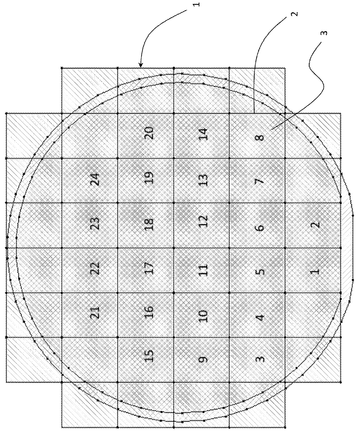
[0012]FIG. 1 illustrates an example layout of reticles 2 on a semiconductor, e.g., CMOS, wafer 1. Reticles 2 numbering 1 to 24 are duplicates of each other post fabrication. However, each reticle 2 may also contain multiple copies of chips 3. The method of the present invention enables the addition of identifiable information to each chip 3 outside of standard semiconductor, e.g., CMOS, processes.
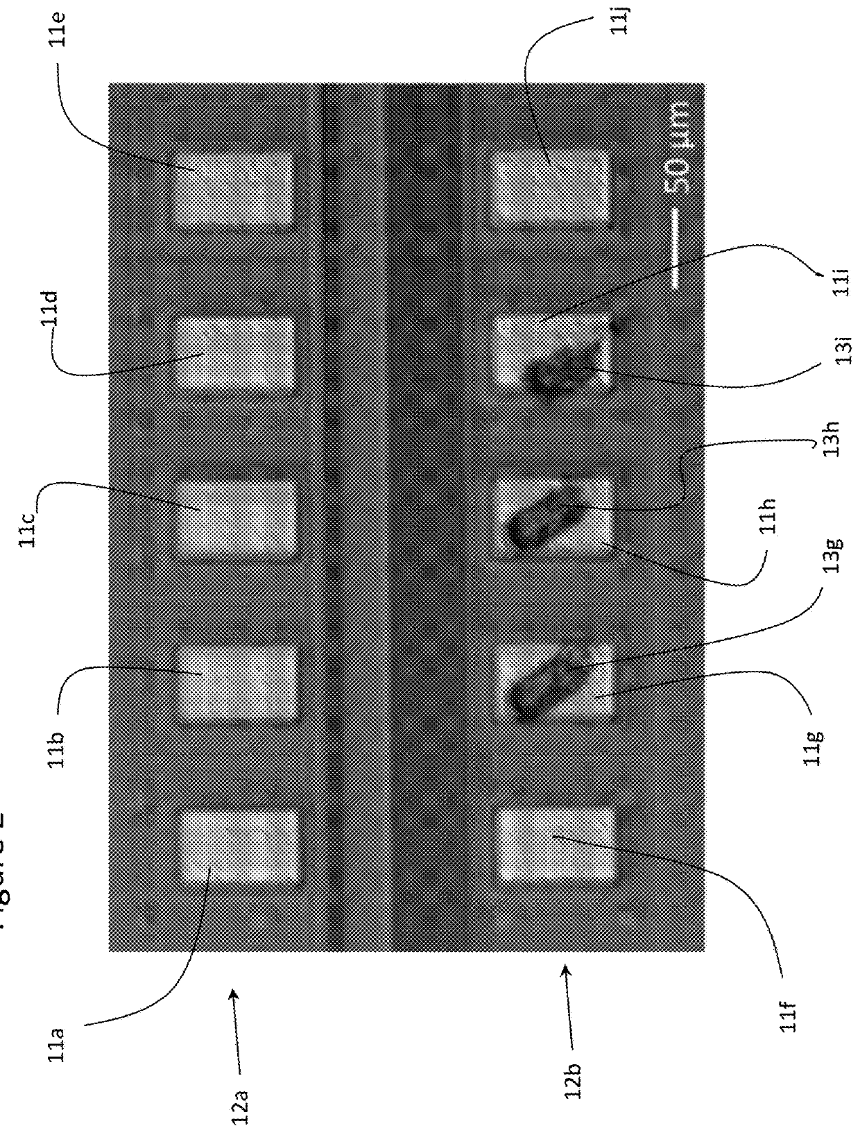
[0013]With reference to FIG. 2, a plurality of extra metal pads 11a to 11j (or collectively as just 11), preferably one or more arrays of metal pads, e.g., 1×N, 2×N, are provided on top of each chip 3 on the semiconductor wafer 1. The arrays of metal pads 11 may include a first row 12a of metal pads comprising at least eight, parallel metal pads 11. Preferably, the arrays of metal pads 11 also includes a second row of metal pads 12b comprising at least eight, parallel metal pads 11. Copper, aluminum, gold, and any other suitable metal pads are typically deposited on top of the semiconductor...
PUM
 Abstract
Description
Claims
Application Information
 - R&D Engineer
- R&D Manager
- IP Professional
- Industry Leading Data Capabilities
- Powerful AI technology
- Patent DNA Extraction
Browse by: Latest US Patents, China's latest patents, Technical Efficacy Thesaurus, Application Domain, Technology Topic.
© 2024 PatSnap. All rights reserved.Legal|Privacy policy|Modern Slavery Act Transparency Statement|Sitemap