Multilayer Wiring Board and Differential Transmission Module
a transmission module and multi-layer technology, applied in waveguides, printed circuit non-printed electric components association, baseband system details, etc., can solve the problems of loss in transmission lines, long transmission distances, etc., and achieve good high-speed signal transmission characteristics
- Summary
- Abstract
- Description
- Claims
- Application Information
AI Technical Summary
Benefits of technology
Problems solved by technology
Method used
Image

Examples
embodiment
[0033]Before describing a multilayer wiring board according to an embodiment, problems of a multilayer wiring board of the related art applied to an ACC connector for differential transmission will be described below. As a paddle board of a connector, a multilayer wiring board where two or more types of layers having different layer thicknesses are laminated is frequently used. In such a multilayer wiring board, in general, since the diameter of a through-hole is formed to be small in a layer with a small layer thickness, the spacing of a through-hole pair corresponding to a wire line pair of differential wire lines (hereinafter, simply referred to as a differential pair of through-holes) becomes a narrow pitch. On the other hand, since the diameter of a through-hole is generally large in a layer having a large layer thickness, the spacing of a differential pair of the through-holes becomes a wide pitch.
[0034]As a result of studies made by the inventors on the problem of the case of...
first embodiment
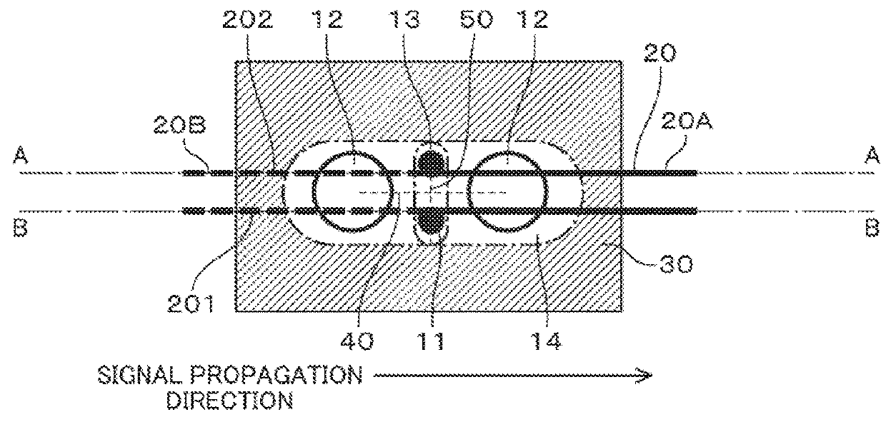
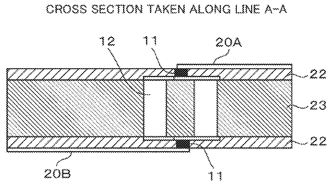
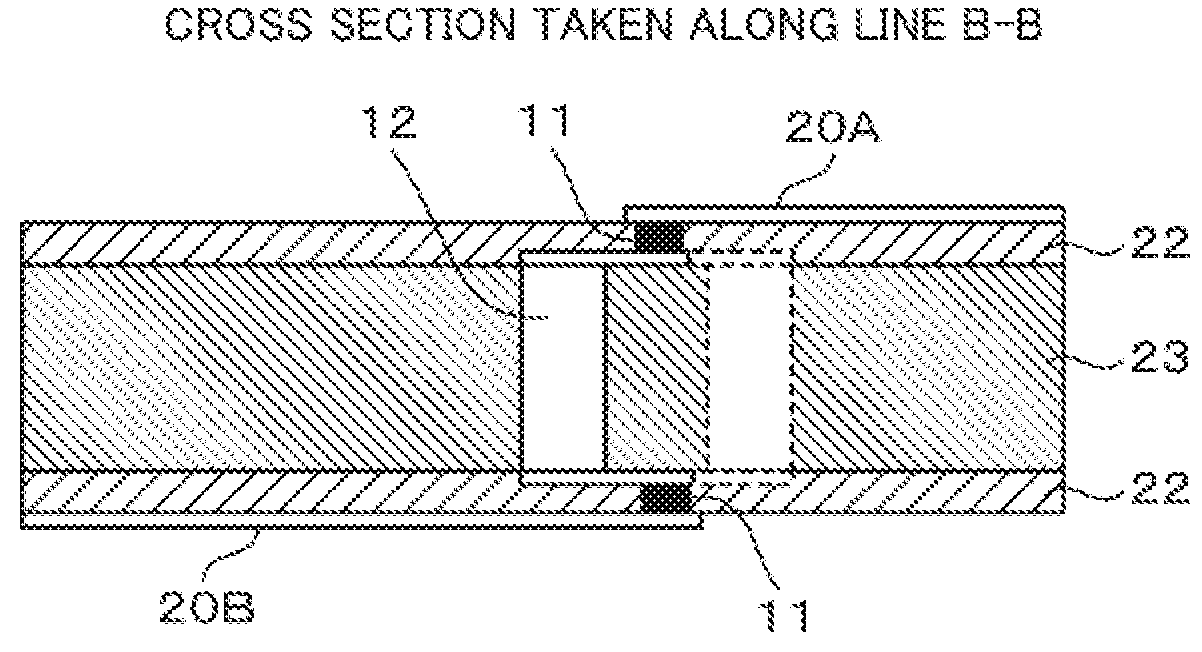
[0039]Hereinafter, a configuration of a multilayer wiring board according to a first embodiment will be described with reference to FIGS. 1 to 5. FIG. 1 is a top view illustrating a through-hole structure of the multilayer wiring board according to the first embodiment. FIGS. 2 and 4 are cross-sectional views taken along line A-A of FIG. 1, and FIG. 3 is a cross-sectional view taken along line B-B of FIG. 1. FIG. 5 is a diagram illustrating a wiring pattern of each layer of the multilayer wiring board illustrated in FIG. 1.
[0040]The multilayer wiring board illustrated in FIGS. 1 to 5 is assumed to be used for a paddle board of a connector related to high-speed wired transmission. As the multilayer wiring board for the paddle board, a resin board laminated with resin layers having different layer thicknesses can be appropriately used. As a result, it is possible to achieve both high density wire line and improved board strength without using high cost materials such as ceramics.
[0041...
second embodiment
[0057]Hereinafter, a configuration of a multilayer wiring board according to a second embodiment will be described with reference to FIGS. 6A, 6B, 7, and 8. FIG. 6A is a diagram illustrating through-holes and clearances formed in the multilayer wiring board according to the first embodiment. FIG. 6B is a diagram illustrating through-holes and clearances formed in the multilayer wiring board according to the second embodiment. FIG. 7 illustrates the relationship between the angle θ between the virtual line 40 connecting the differential pair of the through-hole 12 in the core layer 23 and the line perpendicular to the signal propagation direction of the differential wire line, and Wclr and Lclr. In the first embodiment, the configuration where the through-hole pair 12 of the core layer 23 is arranged so that the virtual line 40 connecting the centers of the differential pair of the through-holes 12 of the core layer 23 is parallel to the signal propagation direction has been describe...
PUM
 Abstract
Description
Claims
Application Information
 - R&D
- Intellectual Property
- Life Sciences
- Materials
- Tech Scout
- Unparalleled Data Quality
- Higher Quality Content
- 60% Fewer Hallucinations
Browse by: Latest US Patents, China's latest patents, Technical Efficacy Thesaurus, Application Domain, Technology Topic, Popular Technical Reports.
© 2025 PatSnap. All rights reserved.Legal|Privacy policy|Modern Slavery Act Transparency Statement|Sitemap|About US| Contact US: help@patsnap.com