Flat liquid crystal display device

Inactive Publication Date: 2018-11-22
TCL CHINA STAR OPTOELECTRONICS TECH CO LTD
View PDF3 Cites 0 Cited by
  • Summary
  • Abstract
  • Description
  • Claims
  • Application Information

AI Technical Summary

Benefits of technology

The present disclosure provides a new pixel structure for a liquid crystal display device that increases the opening ratio and permeability of the display device. The two adjacent pixel structural units are oppositely arranged, and in two adjacent rows of pixel structural units, two pixel structural units in a same column share one common electrode contact hole. This arrangement improves the display quality of high-resolution pixels and enhances the overall performance of the liquid crystal display device.

Problems solved by technology

It can be seen that, the existence of a large number of common electrode contact holes in this array results in a low opening ratio of the liquid crystal display device, thus decreasing the permeability of the liquid crystal display device.

Method used


Image

  • Flat liquid crystal display device
  • Flat liquid crystal display device
  • Flat liquid crystal display device

Examples


Embodiment Construction

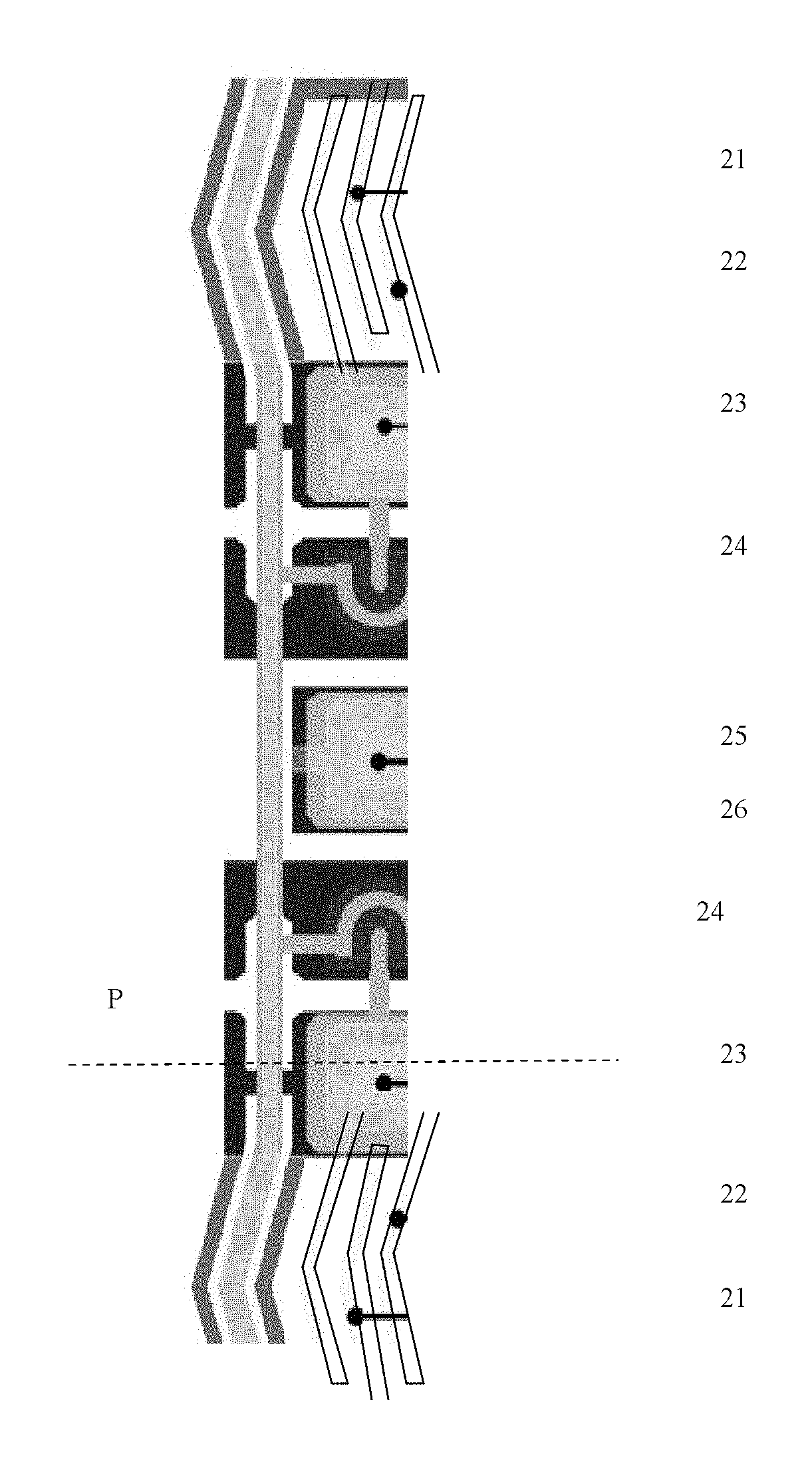
[0028]The present application provides a flat liquid crystal display device. A pixel substrate of the flat liquid crystal display device comprises a plurality of repetitive pixel array units. FIG. 3 is a schematic diagram of a structure of pixel array units according to one embodiment of the present application, in which two adjacent paired pixel array units sharing the same common electrode contact hole are shown. In this diagram, 21 represents a common electrode, 22 represents a pixel electrode, 23 represents a pixel electrode contact hole, 24 represents a scanning line, 25 represents a common electrode contact hole, and 26 represents a data line.

[0029]As shown in FIG. 3, it can be seen that, as observed in a normal direction (i.e., a direction perpendicular to the principal plane) of a display panel, each of the pixel array units comprises: a pixel electrode contact hole 23 in a central region of the pixel array unit; a common electrode 21 and a pixel electrode 22 at one side of ...


PUM


Abstract

Disclosed is a flat liquid crystal display device. A pixel substrate of the flat liquid crystal display device includes a plurality of repetitive pixel array units. As observed in a normal direction of a display panel, each of the pixel array units includes: a pixel electrode contact hole in a central region; a common electrode and a pixel electrode at one side of the pixel electrode contact hole; and a common electrode contact hole at the other side of the pixel electrode contact hole opposite to the common electrode and the pixel electrode. Two adjacent pixel array units share the same common electrode contact hole and are symmetrical about a central cross section of the shared common electrode contact hole. The flat liquid crystal display device is applied to the field of flat liquid crystal display device.

Description

CROSS-REFERENCE TO RELATED APPLICATIONS[0001]The present application claims the priority of Chinese patent application CN 201610799148.5, entitled “Flat liquid crystal display device” and filed on Aug. 31, 2016, the entirety of which is incorporated herein by reference.FIELD OF THE INVENTION[0002]The present disclosure relates to the technical field of liquid crystal display, and in particular, to a flat liquid crystal display device.BACKGROUND OF THE INVENTION[0003]Liquid crystal display device is a most widely used type of flat display device currently, and has gradually become the display device with a high-resolution which is widely used in various electronic devices such as mobile phones, personal digital assistants (PDAs), digital cameras, computer screens or notebook computer screens. With development and advancements in the technologies of liquid crystal display device, people put forward higher requirements for display quality, appearance design, low cost, high permeability...

Claims


Application Information

Patent Timeline
IPC IPC(8): G09G3/34
CPCG09G3/34G02F1/134363G02F1/136227G02F1/136286G02F2201/40
Inventor HAO, SIKUN
Owner TCL CHINA STAR OPTOELECTRONICS TECH CO LTD
Why Eureka
Try Eureka