Methods for forming low temperature semiconductor layers and related semiconductor device structures

a technology of low temperature and semiconductor layers, applied in the direction of semiconductor devices, basic electric elements, electrical equipment, etc., can solve the problems of difficult to get the film growth to completely fill in the gaps, and the film closure may not be possibl

Active Publication Date: 2018-12-06
ASM IP HLDG BV
View PDF0 Cites 241 Cited by
  • Summary
  • Abstract
  • Description
  • Claims
  • Application Information

AI Technical Summary

Problems solved by technology

However, there may be difficulty encountered in trying to get the film growth to completely fil

Method used


Image

  • Methods for forming low temperature semiconductor layers and related semiconductor device structures
  • Methods for forming low temperature semiconductor layers and related semiconductor device structures
  • Methods for forming low temperature semiconductor layers and related semiconductor device structures

Examples


Embodiment Construction

[0013]Although certain embodiments and examples are disclosed below, it will be understood by those in the art that the invention extends beyond the specifically disclosed embodiments and / or uses of the invention and obvious modifications and equivalents thereof. Thus, it is intended that the scope of the invention disclosed should not be limited by the particular disclosed embodiments described below.

[0014]As used herein, the term “substrate” may refer to any underlying material or materials that may be used, or upon which, a device, a circuit or a film may be formed.

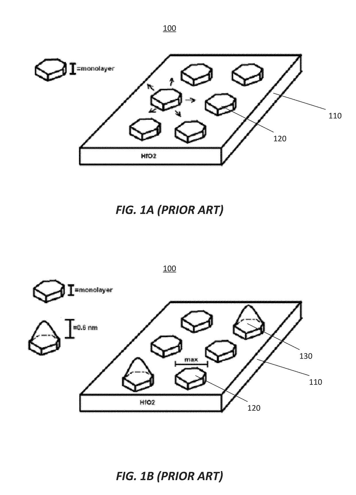
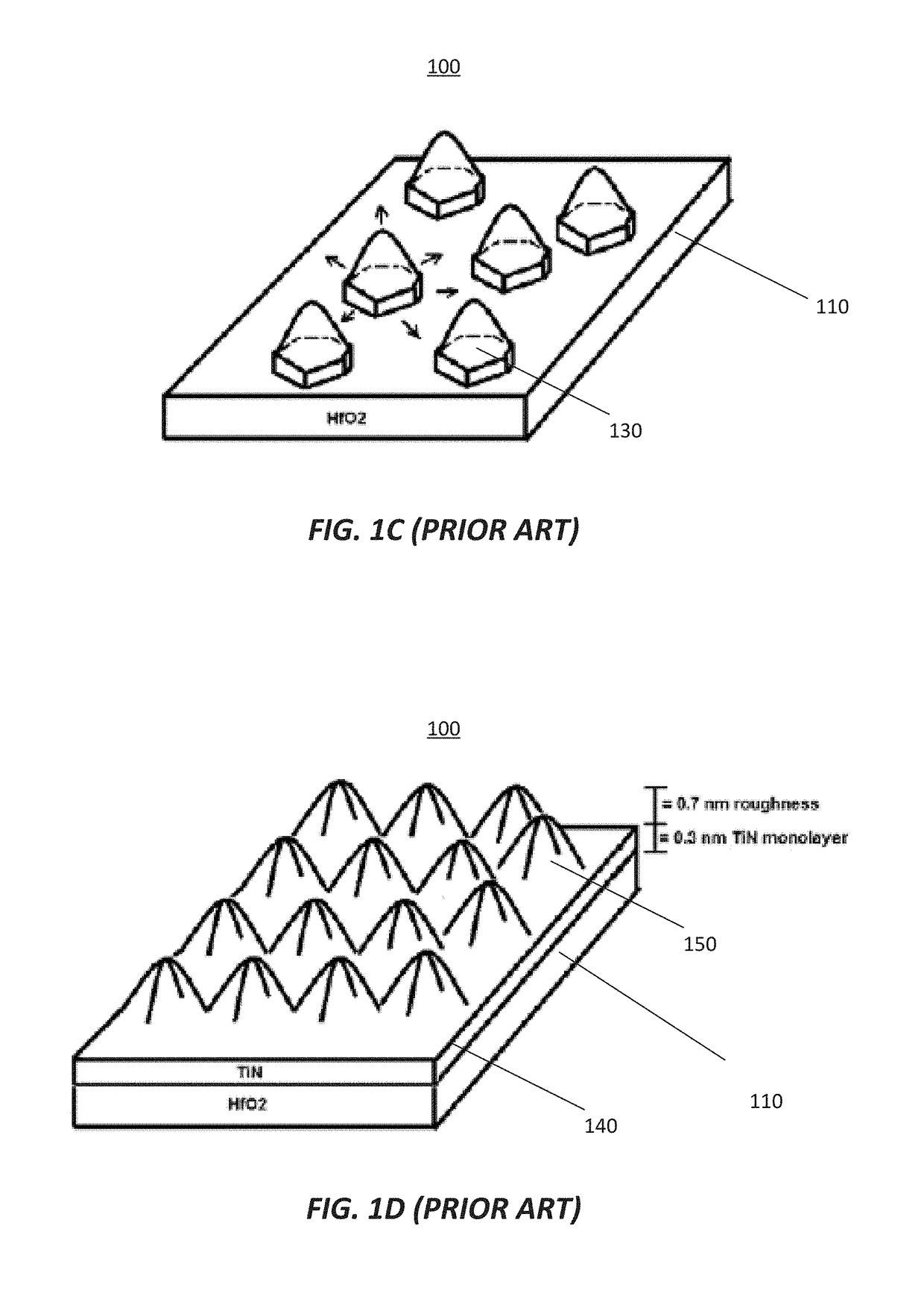
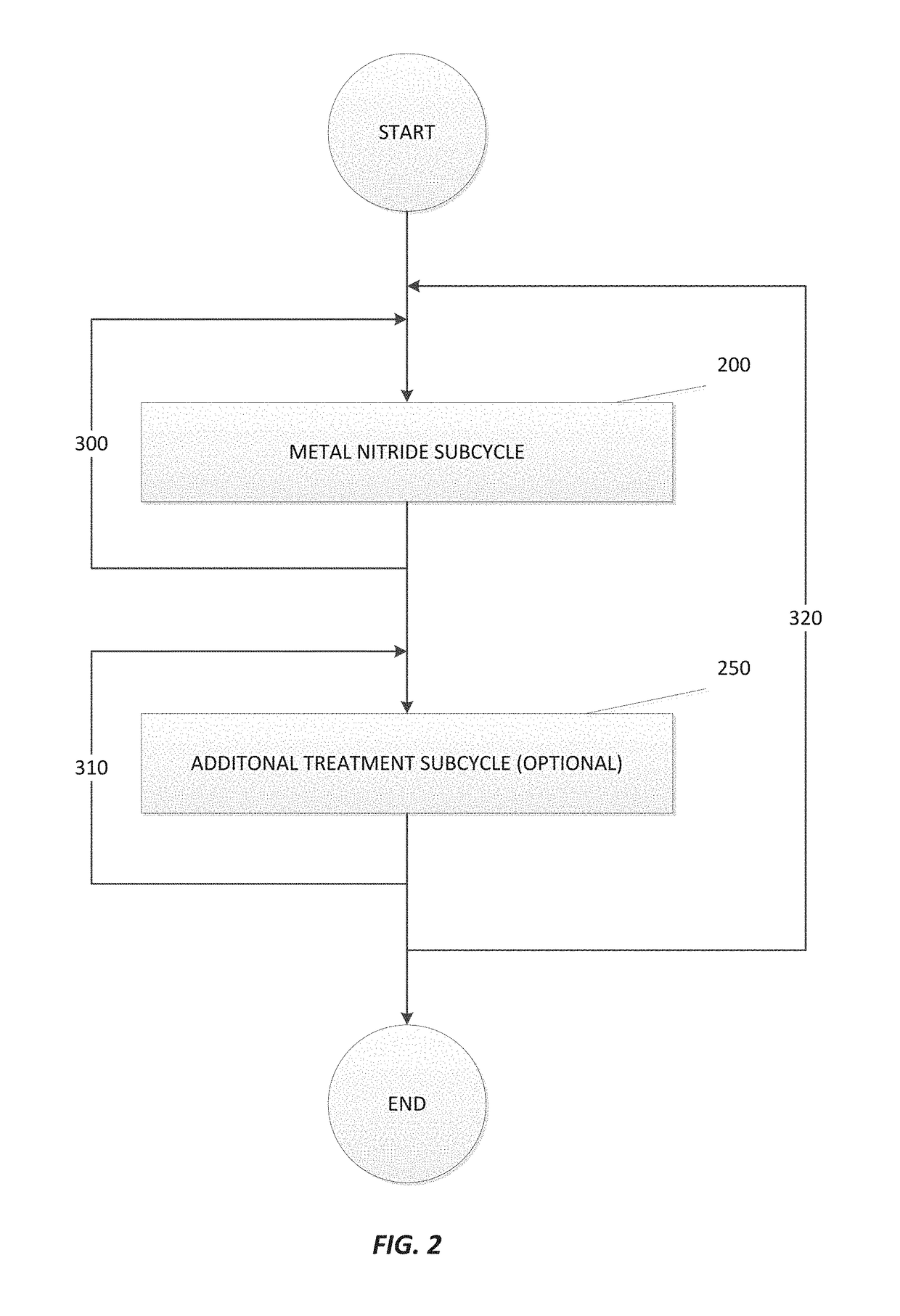
[0015]The embodiments of the disclosure may include methods for forming metal nitride films at low temperatures. The films formed may be amorphous films or crystalline films with a high degree of uniformity. The films formed may be continuous amorphous films. The films may be formed onto a substrate within a reaction chamber. It is an object of the invention to form amorphous films in a manner such that three-dimension...


PUM


Abstract

A method for forming a metal nitride film with good film closure at low temperatures is disclosed. The method may comprise utilizing plasma to form NH and NH2 radicals to allow for the formation of the metal nitride at low temperatures. The method may also comprise flowing an etch gas to result in an amorphous film with uniform thickness. The method may also comprise flowing an alkyl hydrazine to inhibit three-dimensional island growth of the metal nitride film.

Description

CROSS-REFERENCE TO RELATED PATENT APPLICATION[0001]The present disclosure claims the benefit of U.S. Provisional Patent Application No. 62 / 514,585, filed on Jun. 2, 2017 and entitled “METHODS FOR FORMING LOW TEMPERATURE SEMICONDUCTOR LAYERS AND RELATED SEMICONDUCTOR DEVICE STRUCTURES,” which is incorporated herein by reference.FIELD OF INVENTION[0002]The present disclosure generally relates to methods for forming semiconductor layers at low temperatures. Particularly, the present disclosure relates to formation of thin nitride films, such as titanium nitride (TiN), for example. The nitride films are formed in a manner that results in a uniform film due to film closure.BACKGROUND OF THE DISCLOSURE[0003]Nitride films have been formed with many different processes. Some processes have resulted in formation of films through island growth. Island growth may comprise a process in which a plurality of separate film growths initiates, with empty areas between the separate film growths being...

Claims


Application Information

Patent Timeline
IPC IPC(8): H01L21/02
CPCH01L21/0234H01L21/02205H01L21/02389H01L21/02181H01L21/02183H01L21/02186H01L21/02189H01L21/762H01L21/768H01L29/78H01L21/32051
Inventor RAISANEN, PETRIMOUSA, MOATAZ BELLAHHSU, PENG-FU
Owner ASM IP HLDG BV
Why Eureka
Try Eureka