

Apparatus and method for removal of oxide and carbon from semiconductor films in a single processing chamber
- Summary
- Abstract
- Description
- Claims
- Application Information
AI Technical Summary
Benefits of technology
Problems solved by technology
Method used
Image

Examples
Embodiment Construction
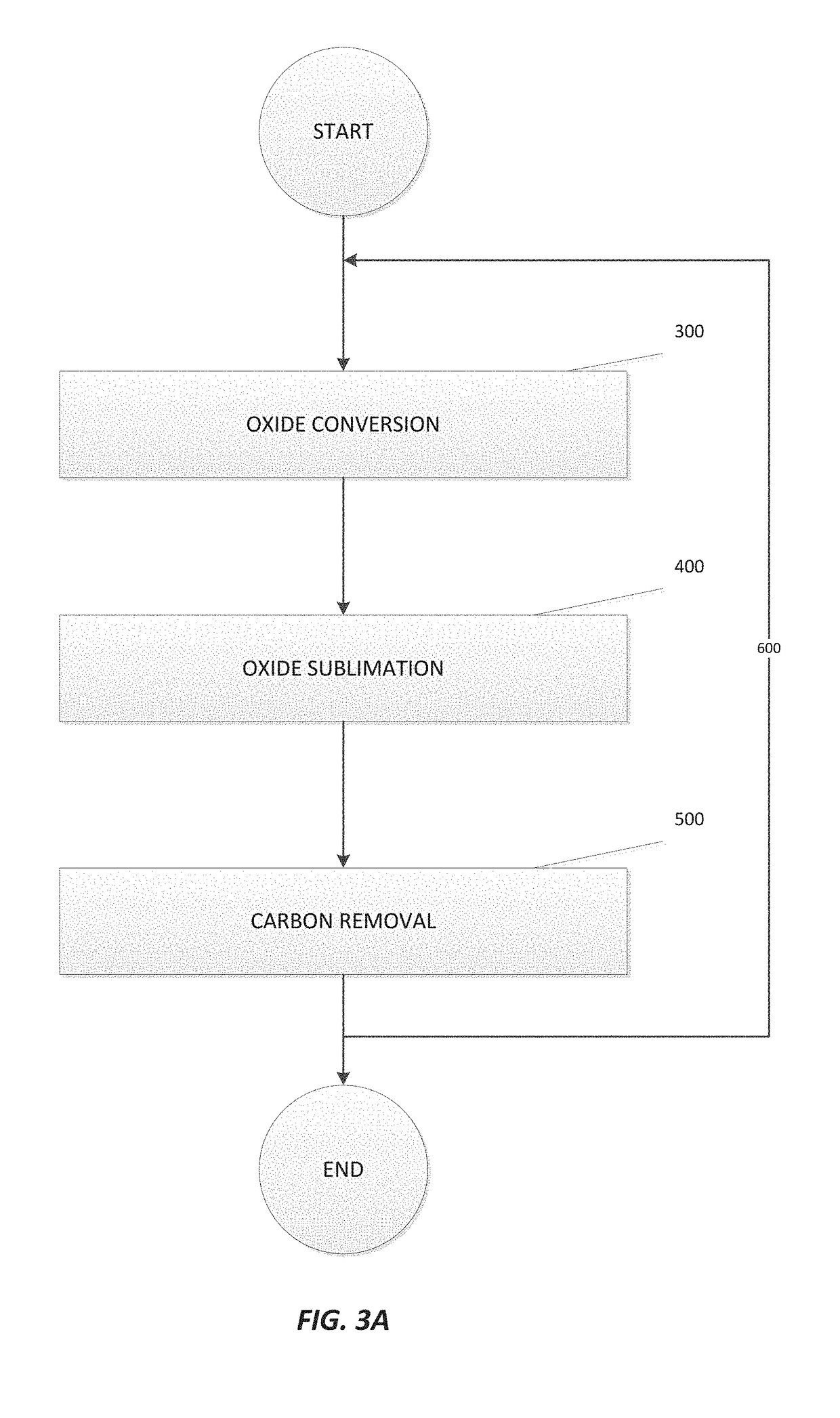
[0014]Although certain embodiments and examples are disclosed below, it will be understood by those in the art that the invention extends beyond the specifically disclosed embodiments and / or uses of the invention and obvious modifications and equivalents thereof. Thus, it is intended that the scope of the invention disclosed should not be limited by the particular disclosed embodiments described below.
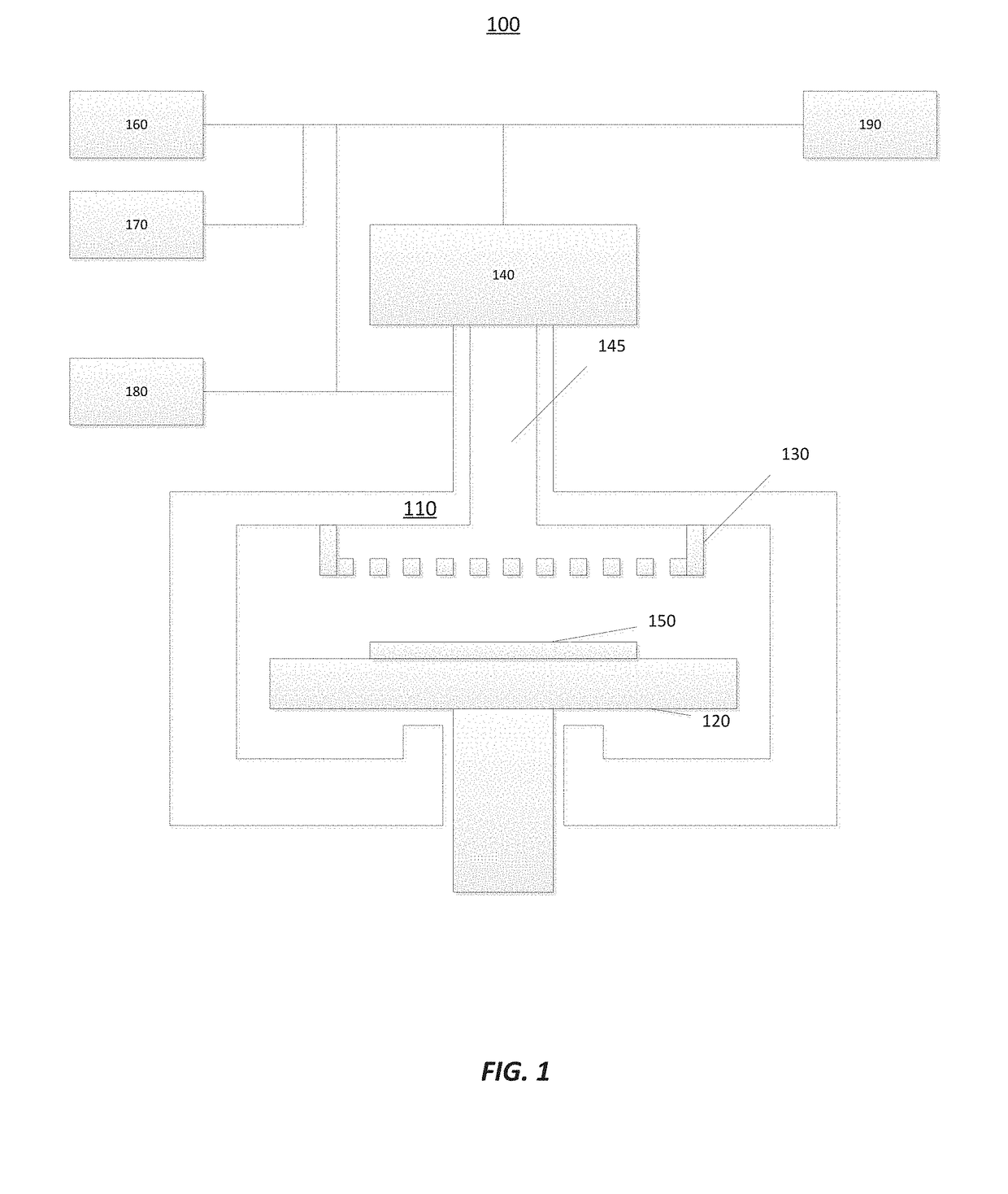
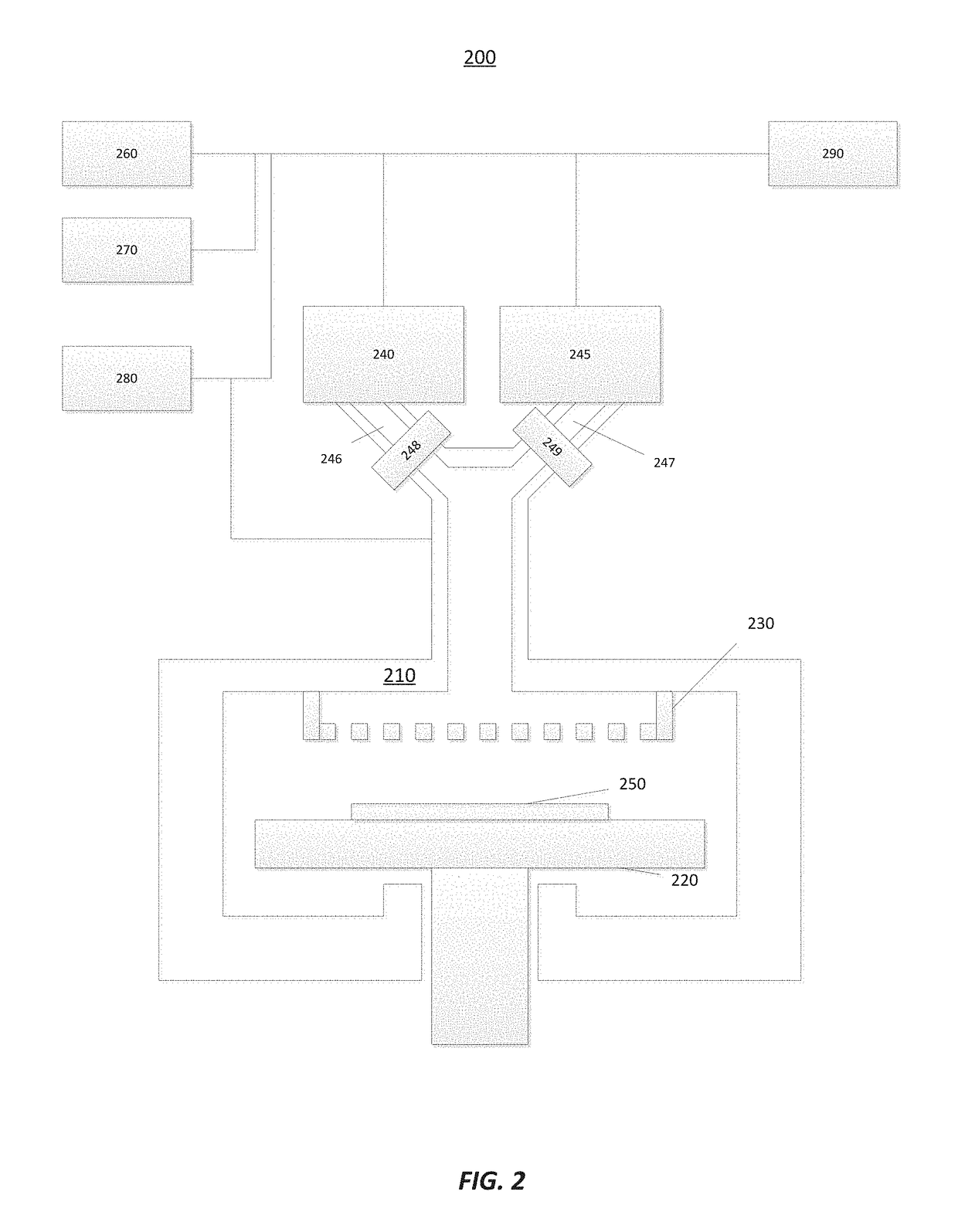
[0015]Embodiments of the invention are directed to a system with a single process chamber having a capability to remove both carbon-based contaminants and oxygen-based contaminants. The embodiments have several advantages over prior approaches including: (1) incorporation of at least one remote plasma unit (RPU) with the ability to generate both hydrogen radicals and fluorine radicals; and (2) compatibility of the process chamber with both hydrogen radicals and fluorine radicals.
[0016]Embodiments of the invention may be used to clean semiconductor substrates made of at least one of the...
PUM
| Property | Measurement | Unit |
|---|---|---|
| Transport properties | aaaaa | aaaaa |
Abstract
Description
Claims
Application Information