
Microfluidic MEMS device with piezoelectric actuation and manufacturing process thereof

Active Publication Date: 2019-01-24
STMICROELECTRONICS SRL
View PDF1 Cites 7 Cited by
  • Summary
  • Abstract
  • Description
  • Claims
  • Application Information

AI Technical Summary

Benefits of technology

This patent describes a new device called a microfluidic MEMS that can be used for inkjet printing. It uses piezoelectric actuation to move ink and is manufactured using a specific process. The technical effect of this patent is the provision of a more efficient and precise inkjet printing device that can be easily manufactured using existing technology.

Problems solved by technology

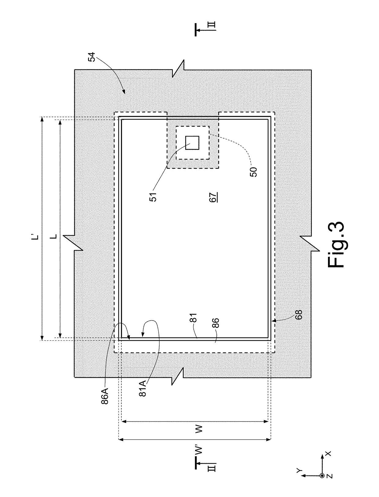
Whereas the control of the thickness of the membrane may be obtained with the usual techniques, it is difficult to obtain the control of the width W of the membrane with such a level of precision by means of the use of the usual fabrication techniques which comprise, for example, deep silicon etch steps.
Indeed, for example in the case of a nominal width W of 80 μm, it is difficult to obtain a variability of less than 0.8 μm, in particular, considering that the etching of the fluid containment chamber (which determines the width of the membrane) is a deep etch, also of 100 μm or more.
Furthermore, potential errors in alignment during the photolithography processes also have an influence on the width W of the membrane and also have an influence on the variability.

Method used


Image

  • Microfluidic MEMS device with piezoelectric actuation and manufacturing process thereof
  • Microfluidic MEMS device with piezoelectric actuation and manufacturing process thereof
  • Microfluidic MEMS device with piezoelectric actuation and manufacturing process thereof

Examples


Embodiment Construction

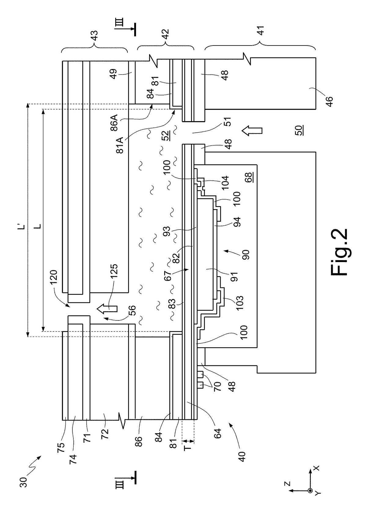
[0028]FIG. 2 shows a single ejector element 40, integrated into a microfluidic device 30.

[0029]The ejector element 40 in FIG. 2 comprises a first, a second and a third region 41, 42, 43, mutually superposed and bonded.

[0030]The first region 41 is formed by a main body 46, made of semiconductor material, for example single-crystal silicon, vertically passing through which, in a direction parallel to the axis Z of a reference coordinate system XYZ, is an inlet channel 50 communicating with an external reservoir (not shown). The main body 46 furthermore forms an actuator chamber 68, disposed laterally to the inlet channel 50 and isolated with respect to the latter.

[0031]The second region 42 is superposed and bonded onto the first region 41 by means of a first layer of adhesive 48. The second region 42 comprises a membrane layer 64, a membrane definition element 81 and a chamber body 86, mutually superposed; for example, the membrane layer 64 and the membrane definition element 81 are m...


PUM


Abstract

The microfluidic device has a plurality of ejector elements. Each ejector element includes a first region, accommodating a first fluid flow channel and an actuator chamber; a second region, accommodating a fluid containment chamber; and a third region, accommodating a second fluid flow channel. The fluid containment chamber is fluidically coupled to the first and to the second fluid flow channels. The second region is formed from a membrane layer, from a membrane definition layer, mechanically coupled to the membrane layer and having a membrane definition opening, and a fluid chamber defining body, mechanically coupled to the membrane definition layer and having a chamber defining opening, with a width greater than the width of the membrane definition opening. The width of the membrane is thus defined by the width of the chamber defining opening.

Description

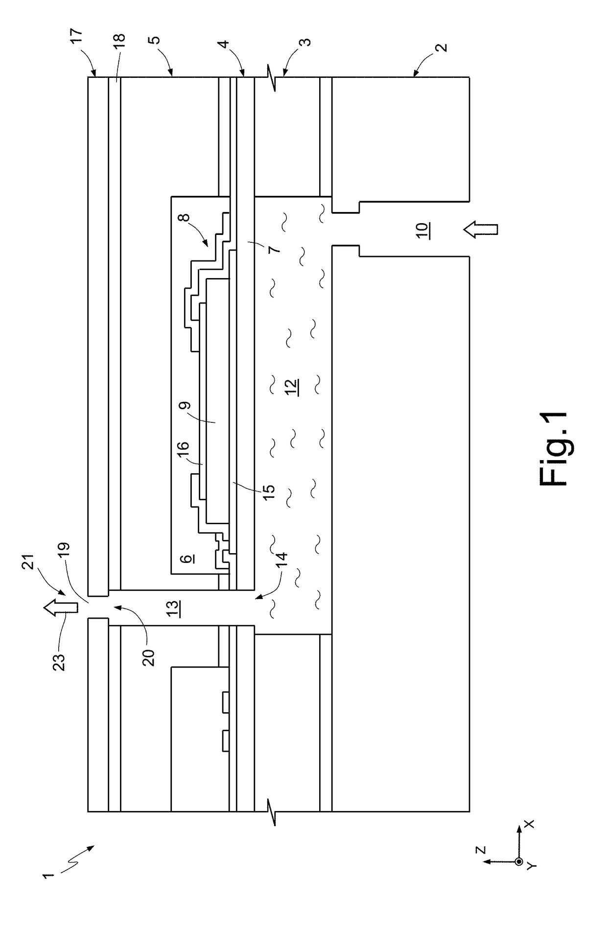
BACKGROUNDTechnical Field[0001]The present disclosure relates to a microfluidic MEMS (“Micro Electro-Mechanical System”) device and to the related manufacturing process.Description of the Related Art[0002]As is known, for the spraying of inks and / or scents, for example perfumes, the use of microfluidic devices with small dimensions, which may be fabricated using microelectronics fabrication techniques, has been proposed.[0003]For example, U.S. Pat. No. 9,174,445 describes a microfluidic device designed for the thermal spraying of ink onto paper.[0004]Another type of microfluidic device designed for the spraying of fluids is based on the piezoelectric principle. In particular, devices with piezoelectric actuation may be classified on the basis of the mode of oscillation—longitudinal or transverse. In the following, reference will be made to devices operating in transverse mode, without the disclosure being limited to this category of devices.[0005]One exemplary embodiment of a microf...

Claims


Application Information

Patent Timeline
IPC IPC(8): B41J2/14B41J2/16
CPCB41J2/14233B41J2/161B41J2/1642B41J2/1626B41J2/015B41J2/135B41J2/14B41J2/1623B41J2/1628B41J2/1631B41J2/1632B41J2002/1437
Inventor GIUSTI, DOMENICOCATTANEO, MAUROPRELINI, CARLO LUIGI
Owner STMICROELECTRONICS SRL
Learn More