Optical module and optical device using same

Active Publication Date: 2019-01-24
SAMSUNG ELECTRONICS CO LTD
View PDF2 Cites 8 Cited by
  • Summary
  • Abstract
  • Description
  • Claims
  • Application Information

AI Technical Summary

Benefits of technology

[0038]According to the present invention, it is possible to effectively overcome the limit of the number of filters in a filter array-based spectrometer and improve the signal restoration capability and resolution of the spectrometer.
[0039]The present invention enables only spectral filters to be coupled to a color filter of a conventional silicon CMOS image sensor or to be applied in a corresponding manner.
[0040]In addition, the

Problems solved by technology

Due to a linear structure whose thickness varies in the length direction, Such an LVF has a limitation in process reproducibility and productivity, and has a disadvantage in that process compatibility with the two-dimensional imaging sensor technology is also insufficient.
On the other hand, since the resolution of a filter array-based spectrometer increases in

Method used


Image

  • Optical module and optical device using same
  • Optical module and optical device using same
  • Optical module and optical device using same

Examples


embodiment 1

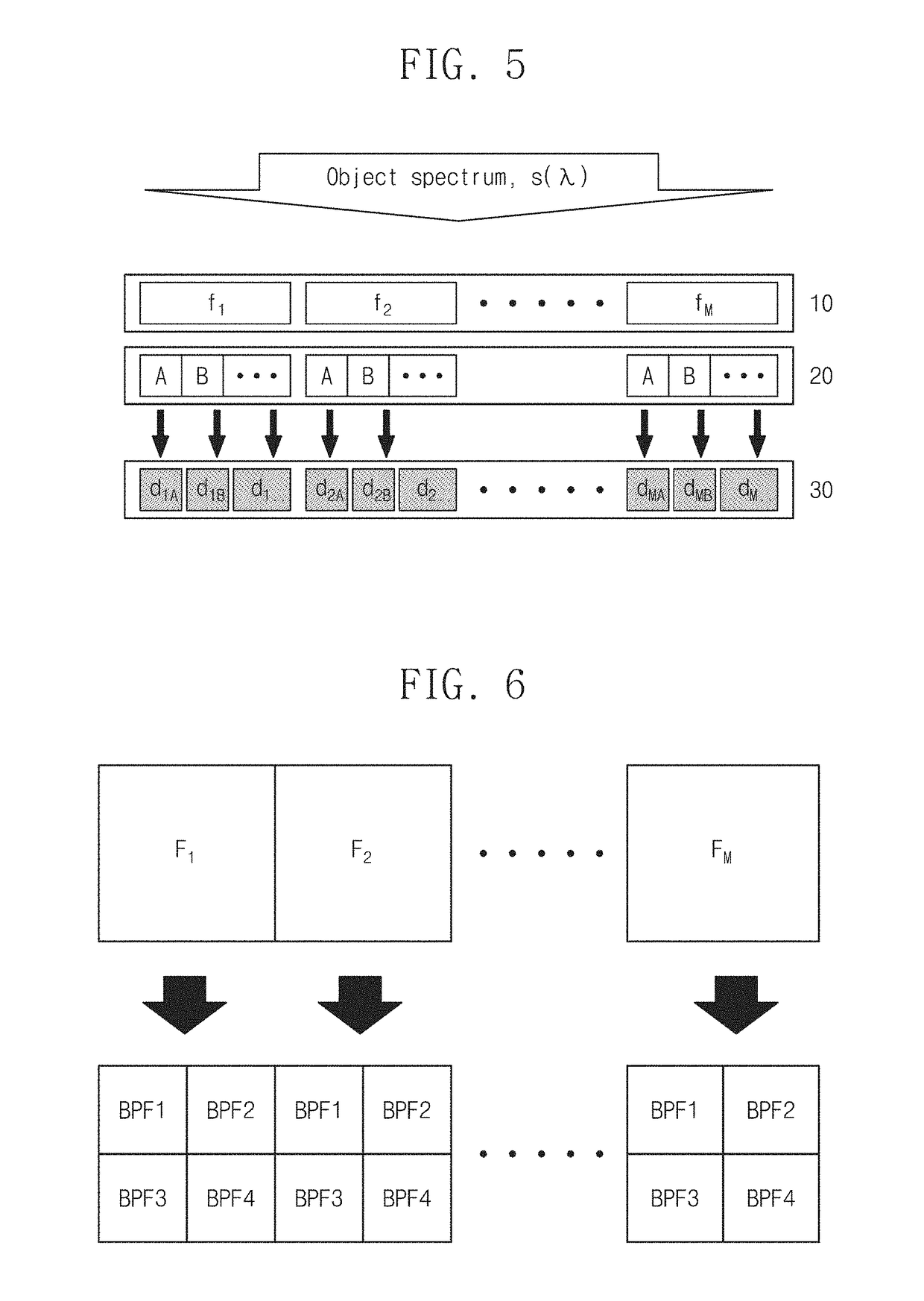
[0071]FIG. 5 is a conceptual diagram of an optical device according to Embodiment 1 of the present invention, and FIG. 6 is a conceptual diagram of a combination structure of a spectral filter and a band-limited filter in an optical device.

[0072]The optical device includes a spectral filter 10, an optical detection unit 30 for detecting light passing through the spectral filter 10, and a band-limited filter 20. The band-limited filter 20 has a wavelength region B smaller than the wavelength band A designed to be measured by the spectral filter 10 as described above.

[0073]Referring to FIG. 6, in the arrangement structure of the band-limited filters 20 corresponding to the unit spectral filters F1, F2, F3 . . . of the spectral filter, a plurality of band-limited filter sets BPF1, BPF2, BPF3, and BPF4 correspond to a unit spectral filter. However, the present invention is not limited thereto and various modifications are possible. That is, unit band-limited filters per unit spectral fi...

embodiment 2

[0085]FIG. 7 is a perspective view of an optical device showing a configuration in which a band-limited filter used as a band-limited filter in the structure of Embodiment 1 is replaced with an RGB color filter of a silicon CMOS image sensor according to Embodiment 2 of the present invention. FIG. 8 is a conceptual diagram showing that four unit RGB color filters for one unit spectral filter are corresponded.

[0086]An advantage of this embodiment is that it is possible to easily construct a structure for coupling a spectral filter array thereon without removing the color filter of a commercially available silicon CMOS image sensor. In this case, the color filter 200 of the CMOS image sensor performs a function similar to the band-limited filter described above. That is, the color filter 200 has a wavelength region B that is smaller than the wavelength band A to be measured in the spectral filter 100.

[0087]On the other hand, according to this embodiment, four unit color filters are sh...

embodiment 3

[0102]FIG. 16 is a conceptual view for explaining signal processing of the optical device according to the third embodiment of the present invention, FIG. 17 is a perspective view of the present optical device, and FIG. 18 shows a structure of a spectral filter and a band-limited filter in the present optical device.

[0103]The optical device includes a spectral filter 50 consisting of unit spectral filters, an optical detection unit 60 for detecting light passing through the spectral filter, and a band-limited filter 40, which is a band-limited filter.

[0104]In relation to the band-limited filter 40, the entire may be formed so as to cover the entire spectral filter as shown in FIGS. 11 and 12, and a plurality of band-pass filters may be arranged as a set. In relation to the band-pass filter set, it is possible that each of the unit band transmission filters transmits the same wavelength band, and that they transmit different wavelength bands.

[0105]This structure is advantageous when ...


PUM


Abstract

The present invention provides an optical device including a spectral filter and an optical detection unit for detecting light passing through the spectral filter. A band-limited filter is provided on the path of light.

Description

CROSS-REFERENCE TO RELATED APPLICATIONS[0001]This U.S. non-provisional patent application claims priority under 35 U.S.C. § 119 of Korean Patent Application Nos. 10-2016-0110799, filed on Aug. 30, 2016, and 10-2017-0053895, filed on Apr. 26, 2017, the entire contents of which are hereby incorporated by reference.TECHNICAL FIELD[0002]The present disclosure relates to a filter array type spectrometer, and more particularly, to an optical module including a band-limiting filter in a spectral filter for signal restoration and resolution enhancement in object spectrum restoration, and an optical device using the optical module.BACKGROUND ART[0003]Spectroscopic instruments, which analyze the intrinsic optical spectrum of a material, are widely used to measure color or molecular bonding of objects in a wideband wavelength range from visible light to infrared band. Conventionally, it has been utilized as a bench top type organic / inorganic substance analyzing instrument such as a UV-VIS-NIR ...

Claims


Application Information

Patent Timeline
IPC IPC(8): G02B5/28G05B23/02H01L27/146
CPCG02B5/28G05B23/02H01L27/14645H01L27/1463H01L27/14621G02B5/201G02B6/29389G02B5/288G05B23/0254
Inventor LEE, KYEONG SEOKHWANG, GYU WEONKIM, WON MOKKIM, IN HOKIM, HYUN CHUL
Owner SAMSUNG ELECTRONICS CO LTD
Why Eureka
Try Eureka