
Wafer processing method

a processing method and wafer technology, applied in the field of wafer processing methods, can solve the problems of long processing time, and achieve the effects of reducing the width of the division line, reducing the number of chips obtainable per wafer, and reducing productivity

Active Publication Date: 2019-01-24
DISCO CORP
View PDF0 Cites 5 Cited by
  • Summary
  • Abstract
  • Description
  • Claims
  • Application Information

AI Technical Summary

Benefits of technology

The present invention provides a wafer processing method that increases the number of chips per wafer and enhances the strength of the chips by forming division lines inside the wafer without needing large width division lines. The method also includes a thinning step to facilitate the formation of cracks in the wafer that can be used to separate the device layers. Additionally, this method eliminates the need for a cutting blade, reducing the number of chips lost during the process. Overall, this method improves the efficiency and effectiveness of the wafer processing process.

Problems solved by technology

In addition, while there is also a method in which the adhesive film is ruptured by laser dicing, a long processing time is required where the chip size is small.

Method used


Image

  • Wafer processing method
  • Wafer processing method
  • Wafer processing method

Examples


Embodiment Construction

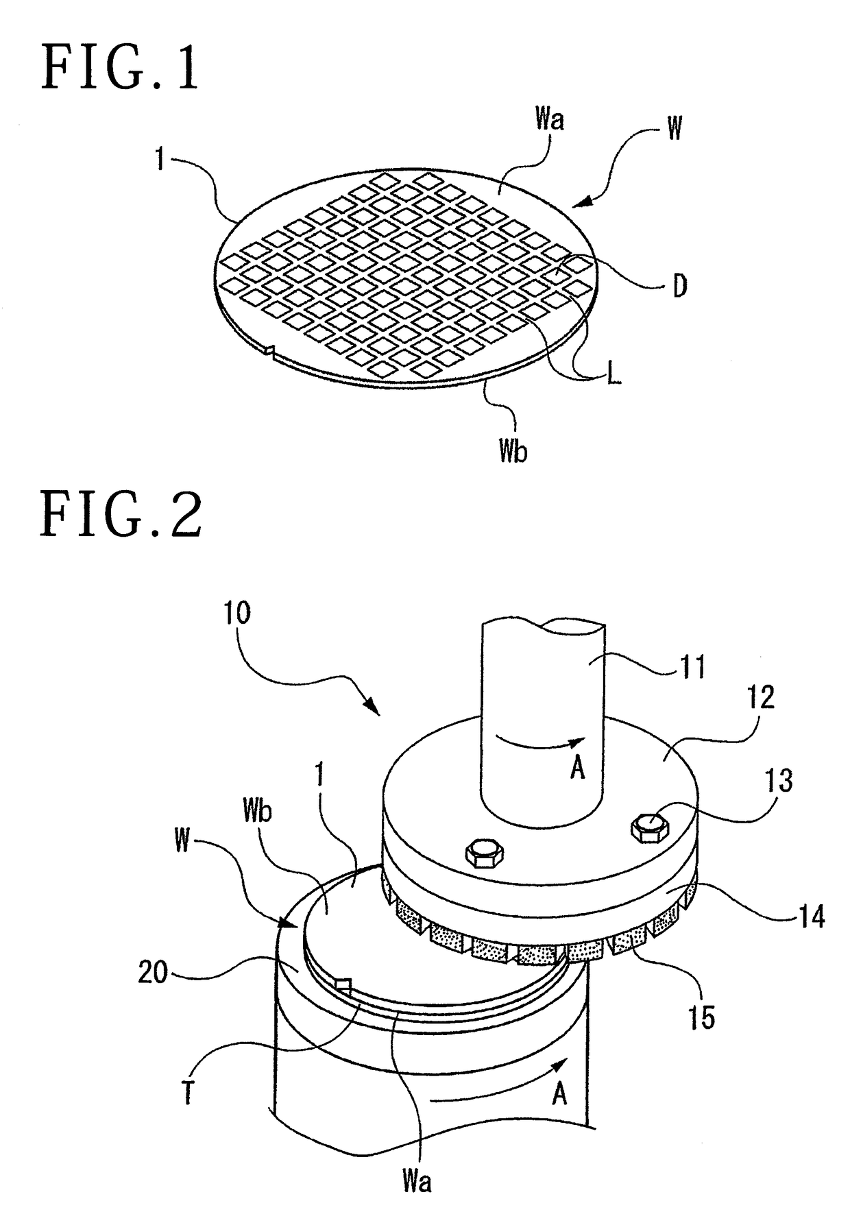
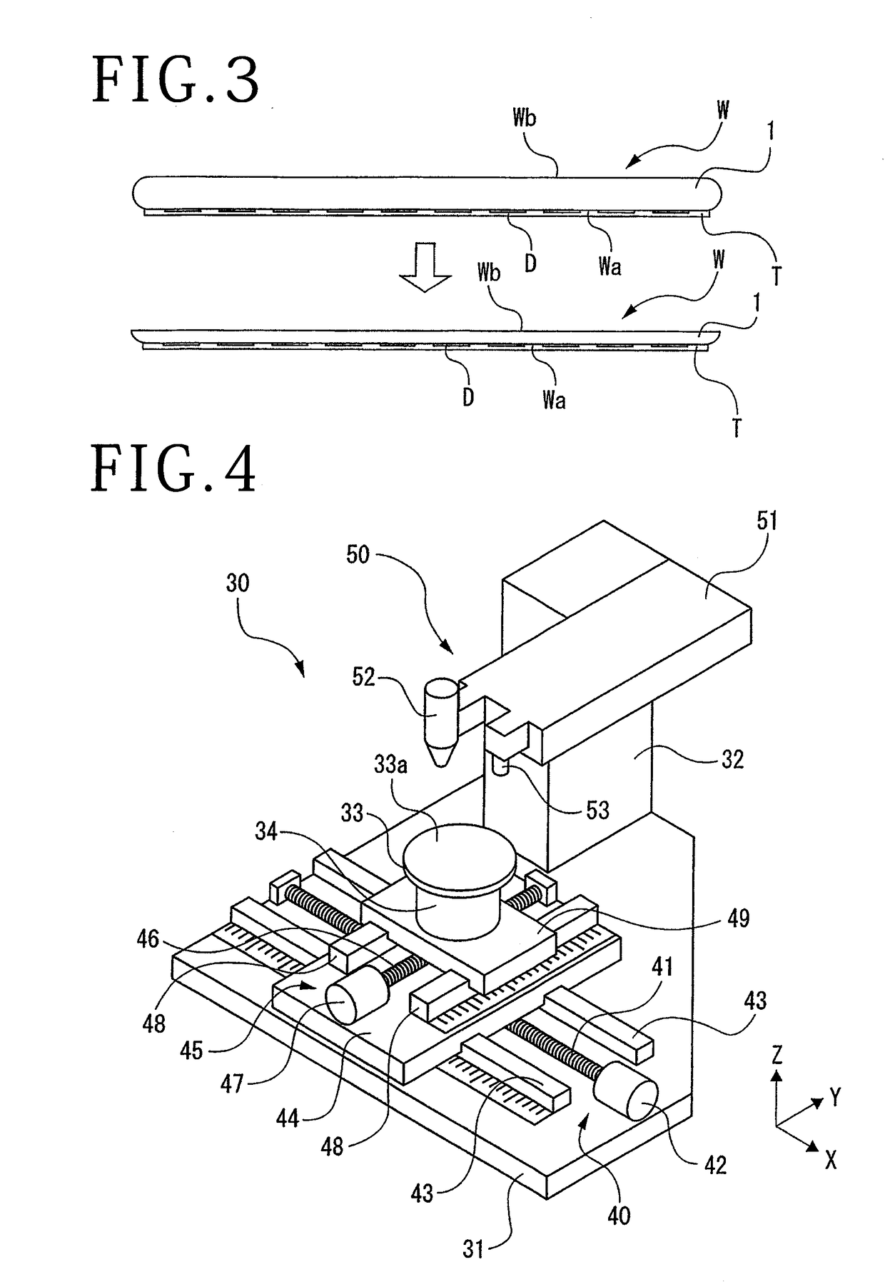
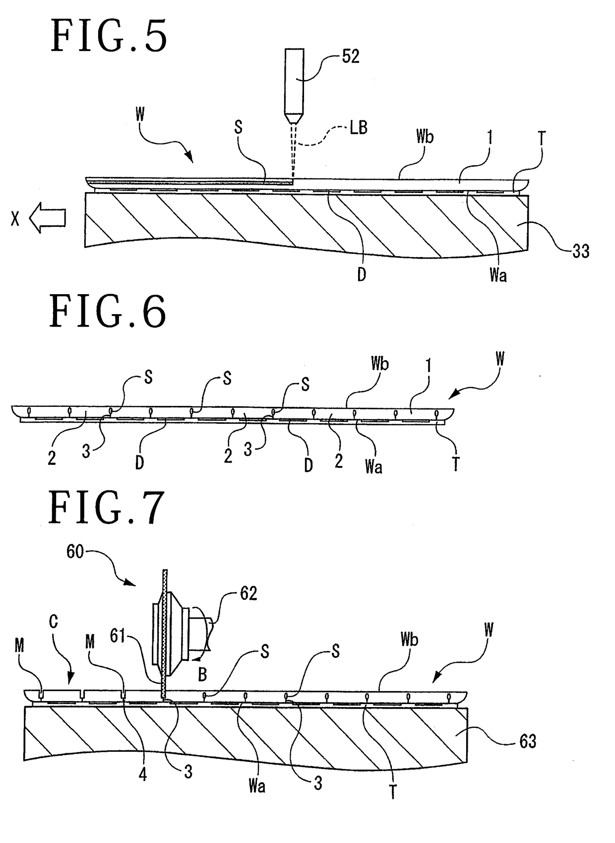
[0025]A wafer W shown in FIG. 1 is an example of a circular plate-shaped workpiece, and it includes a substrate 1, and a device layer formed with devices D such as large scale integrated circuits (LSIs) in respective regions partitioned by a plurality of division lines (streets) L intersecting on a front surface Wa of the substrate 1. A back surface Wb on a side opposite to the front surface Wa of the substrate 1 is a work surface to be subjected to grinding or the like. A wafer processing method for dividing the wafer W into individual chips will be described below.

(1) Thinning Step

[0026]First, using a grinding unit 10 shown in FIG. 2, the back surface Wb of the wafer W is ground to thin the wafer W to a finished thickness. The grinding unit 10 includes a spindle 11 rotationally driven by a motor, a mount 12 fixed to a lower end of the spindle 11, a grinding wheel 14 detachably mounted to the mount 12 by a plurality of screws 13, and a plurality of grindstones 15 firmly attached, i...


PUM

PropertyMeasurementUnit
thicknessaaaaaaaaaa
wavelengthaaaaaaaaaa
thicknessaaaaaaaaaa

Abstract

A method of processing a wafer includes a laser beam applying step of applying a laser beam to the wafer to form modified layers in the inside of the wafer along division lines and to extend device layer splitting cracks from the modified layers to the front surface of the wafer. After the laser beam applying step is performed, a cutting step of cutting the wafer is performed by a cutting blade from the back surface side to form cut grooves and to remove the modified layers. Therefore, the modified layers are not left on chips, and the die strength of the chips is enhanced.

Description

BACKGROUND OF THE INVENTIONField of the Invention[0001]The present invention relates to a method of processing a wafer that has a substrate and a device layer formed with devices in respective regions partitioned by a plurality of division lines (streets) intersecting on a front surface of the substrate.Description of the Related Art[0002]As a method for dividing a wafer into individual chips, there is, for example, a method in which a laser beam is applied to the inside of the wafer along division lines to form modified layers in the inside of the wafer, and then an external force is applied along the division lines to divide the wafer, with the modified layers as division starting points (see, for example, Japanese Patent No. 3408805). As an apparatus for applying an external force to the wafer, there is an expanding apparatus that can expand in plane directions a wafer supported by an annular frame through an expandable tape (see, for example, Japanese Patent Laid-open No. 2007-2...

Claims


Application Information

Patent Timeline
Patent Type & Authority Applications(United States)
IPC IPC(8): H01L21/78H01L21/304
CPCH01L21/78H01L21/304H01L21/76H01L21/67092H01L21/02016B23K26/53B23K2103/56
Inventor SUGIYA, TETSUKAZU
Owner DISCO CORP
Learn More