
Growth of iii-nitride semiconductors on thin van der waals buffers for mechanical lift off and transfer

a technology of iii-nitride semiconductors and buffer materials, which is applied in the direction of semiconductor/solid-state device manufacturing, basic electric elements, electric apparatus, etc., can solve the problems of low cost, large area, and lack of high-quality native substrates for epitaxial growth

Active Publication Date: 2019-01-31
THE UNITED STATES OF AMERICA AS REPRESETNED BY THE SEC OF THE AIR FORCE
View PDF2 Cites 14 Cited by
  • Summary
  • Abstract
  • Description
  • Claims
  • Application Information

AI Technical Summary

Benefits of technology

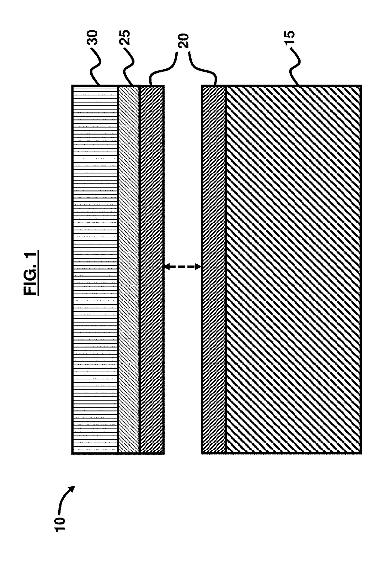
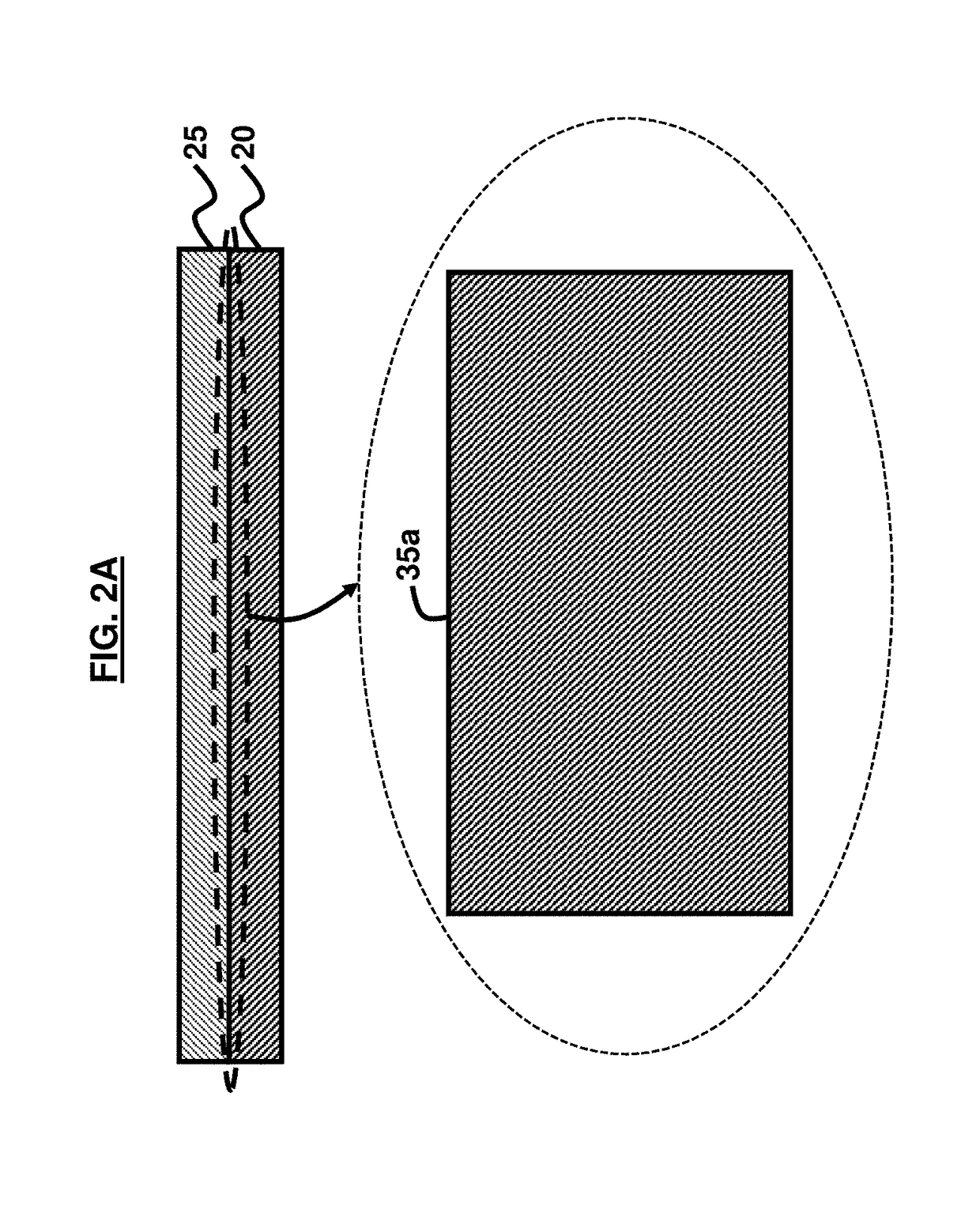
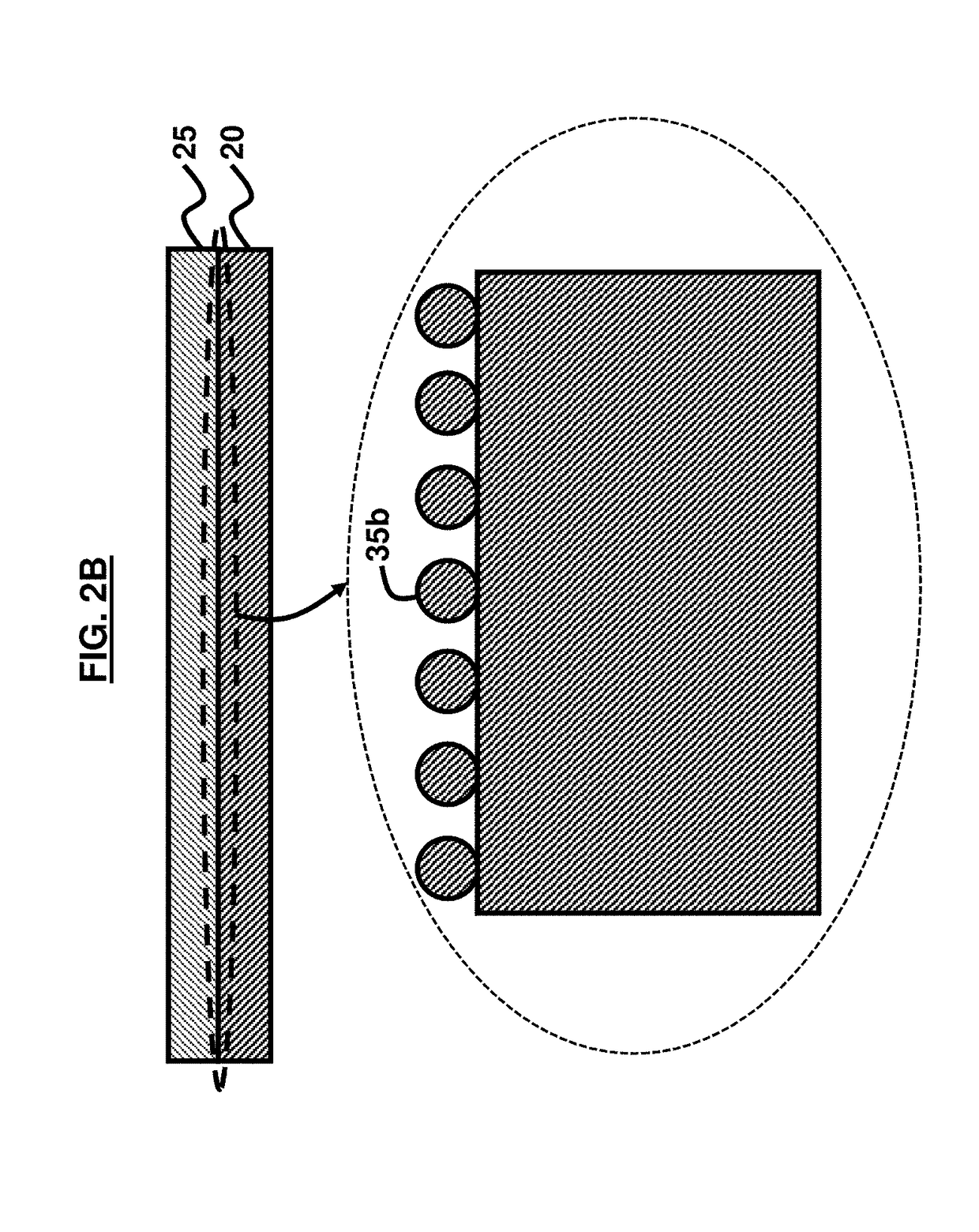
The patent text describes a semiconductor device and a method for growing a semiconductor layer on a substrate. The device includes a mechanical release layer with a specific material roughness and thickness that is attached to the substrate. A nucleation layer is then deposited on top of the release layer, followed by a semiconductor layer that is attached to the nucleation layer. The bonding strength between the semiconductor layer and the substrate is controlled by the material roughness and thickness of the release layer. The method involves depositing a vdW buffer layer with specific material roughness and thickness on the substrate, growing a nucleation layer on the vdW buffer layer, and growing the semiconductor layer on the nucleation layer. The bonding strength between the semiconductor layer and the substrate can be controlled by adjusting the material roughness and thickness of the vdW buffer layer.

Problems solved by technology

One major limitation to producing these materials and devices is the lack of low cost, large area, and high quality native substrates for their epitaxial growth.

Method used


Image

  • Growth of iii-nitride semiconductors on thin van der waals buffers for mechanical lift off and transfer
  • Growth of iii-nitride semiconductors on thin van der waals buffers for mechanical lift off and transfer
  • Growth of iii-nitride semiconductors on thin van der waals buffers for mechanical lift off and transfer

Examples


Embodiment Construction

[0046]Embodiments of the disclosed invention, its various features and the advantageous details thereof, are explained more fully with reference to the non-limiting embodiments that are illustrated in the accompanying drawings and detailed in the following description. Descriptions of well-known components and processing techniques are omitted to not unnecessarily obscure what is being disclosed. Examples may be provided and when so provided are intended merely to facilitate an understanding of the ways in which the invention may be practiced and to further enable those of skill in the art to practice its various embodiments. Accordingly, examples should not be construed as limiting the scope of what is disclosed and otherwise claimed.

[0047]The growth of III-nitride materials, films, and device structures on 2D materials, such as graphene and boron nitride (BN), is attractive for a number of applications including high brightness light emitting diodes (LEDs) and high power high freq...


PUM


Abstract

A semiconductor device includes a mechanical release layer, such as a van der Waals buffer layer, with a predetermined material roughness and thickness adjacent to a first substrate; a nucleation layer adjacent to the mechanical release layer; and a first semiconductor layer attached to the nucleation layer. The first semiconductor layer, the nucleation layer, and a portion of the mechanical release layer are releasably connected to the first substrate. The predetermined material roughness and thickness of the mechanical release layer determines a bonding strength of the first semiconductor layer to the first substrate. The semiconductor device may include an aluminum nitride insert layer adjacent to the first semiconductor layer; an aluminum gallium nitride barrier layer adjacent to the aluminum nitride insert layer; and a second semiconductor layer adjacent to the aluminum gallium nitride barrier layer. The semiconductor device may include a second substrate attached to the released first semiconductor layer.

Description

CROSS-REFERENCE TO RELATED APPLICATION(S)[0001]This application claims the benefit of U.S. Provisional Patent Application No. 62 / 536,524 filed on Jul. 25, 2017, which is incorporated herein by reference in its entirety.GOVERNMENT INTEREST[0002]The invention described herein may be manufactured and used by or for the Government of the United States for all government purposes without the payment of any royalty.BACKGROUNDField of the Invention[0003]The embodiments herein generally relate to epitaxial growth processes for semiconductor devices, and more particularly to growing group III-nitride semiconductors on thin van der Waals buffer materials for mechanical separation from the growth substrate.Background of the Invention[0004]Group III-nitride materials are of interest for producing electronic and opto-electronic integrated circuits that can be found in many electronic devices including solid state lighting, RADARs, and two-dimensional (2D) imaging arrays. For example, devices bas...

Claims


Application Information

Patent Timeline
Patent Type & Authority Applications(United States)
IPC IPC(8): H01L21/02H01L21/78
CPCH01L21/02502H01L21/7806H01L21/0254H01L21/02444H01L21/02458H01L21/0242H01L21/02485H01L21/0262H01L21/02664H01L21/02505
Inventor SNURE, MICHAEL R.SIEGEL, GENE P.PADUANO, QING
Owner THE UNITED STATES OF AMERICA AS REPRESETNED BY THE SEC OF THE AIR FORCE
Learn More