Method for improved semiconductor processing equipment tool pedestal / pad vibration isolation and reduction

a technology of vibration isolation and semiconductor processing equipment, applied in the field of semiconductor and similar high-precision processing facilities, can solve the problems of low production yield rate in semiconductor fabrication, unfavorable replacement of all support tools with vibration specifications for new key production tools, and contributing to unwanted vibration frequencies. , to achieve the effect of improving vibration isolation and reduction, improving vibration control and protection

Active Publication Date: 2019-02-07
SK COMML CONSTR INC
View PDF5 Cites 1 Cited by
  • Summary
  • Abstract
  • Description
  • Claims
  • Application Information

AI Technical Summary

Benefits of technology

[0021]The disclosed subject matter provides for improved vibration control and protection for semiconductor fabrication equipment. Additionally, the present disclosure provides a method and system for improved semiconductor processing equipment vibration isolation and reduction using an integrated system for eliminating vibration conduction paths throughout the fabrication facility.

Problems solved by technology

Low frequency vibration may affect production tools such as lithograph tools and, thereby, lower production yield rate in semiconductor fabrication.
Many lines and pipes from pumps, compressors, chillers attach to pedestals under these tools without vibration isolation support mounts, contributing to unwanted vibration frequencies.
Due to cost and installation time, only critical semiconductor production tools are equipped with vibration controlled and / or active isolation or vibration dampening tool pedestals and pads; most tools rely on their built in passive vibration isolation systems for vibration control.
Most semiconductor fabrication facilities are routinely remodeled, modified, and repurposed multiple times to accommodate new technology due to enormous building cost and prolonged build time.
However, new critical tools are usually operating in conjunction with older support tools with outdated vibration specifications.
Economically, replacing all support tools with matching vibration specifications for new key production tools is not feasible.
Rewiring and / or retrofitting / adding shielding to all EMI emitting electrical lines around EMI sensitive tools to meet new EMI tolerance requirements are not economically feasible.
Disturbance from EMI may degrade the performance of semiconductor processing tools, largely affecting production yield rate.
For such reason, most of the modern semiconductor fabrication facilities prohibit the personal use of radio, mobile, and other external EMI producing devices inside the FAB.
Vibration causes deflection and deflection causes damaging effects to the costly high-precision machine tools.
This, in turn, reduces the production yield rate.

Method used


Image

  • Method for improved semiconductor processing equipment tool pedestal / pad vibration isolation and reduction
  • Method for improved semiconductor processing equipment tool pedestal / pad vibration isolation and reduction
  • Method for improved semiconductor processing equipment tool pedestal / pad vibration isolation and reduction

Examples


Embodiment Construction

[0062]The detailed description set forth below, in connection with the appended drawings, is intended as a description of exemplary embodiments in which the presently disclosed process can be practiced. The term “exemplary” used throughout this description means “serving as an example, instance, or illustration,” and should not necessarily be construed as preferred or advantageous over other embodiments. The detailed description includes specific details for providing a thorough understanding of the presently disclosed method and system. However, it will be apparent to those skilled in the art that the presently disclosed process may be practiced without these specific details. In some instances, well-known structures and devices are shown in block diagram form in order to avoid obscuring the concepts of the presently disclosed method and system.

[0063]In the present specification, an embodiment showing a singular component should not be considered limiting. Rather, the subject matte...


PUM

PropertyMeasurementUnit
frequenciesaaaaaaaaaa
frequencyaaaaaaaaaa
frequencyaaaaaaaaaa

Abstract

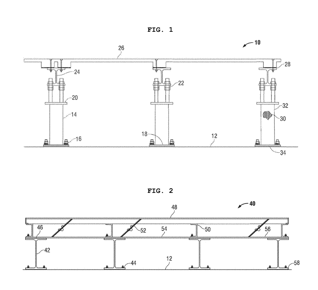
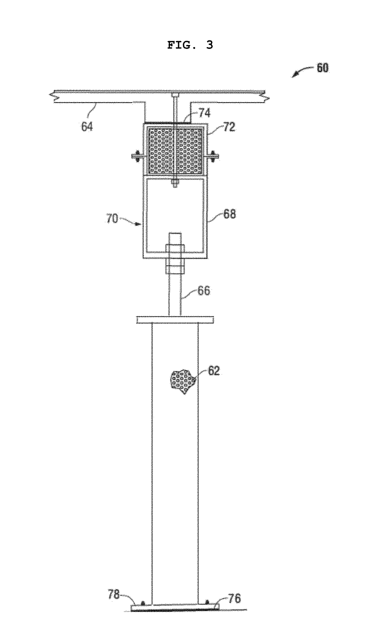
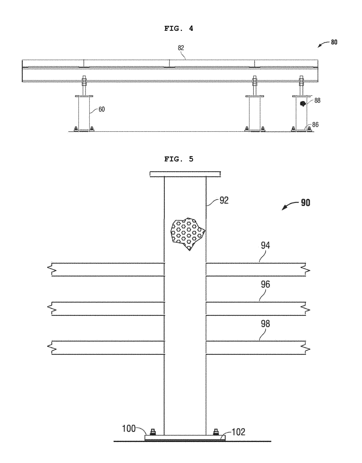
The present disclosure provides a method, system, and fabrication facility that eliminates or substantially reduces process-limiting vibrations within a high-precision device manufacturing facility, wherein an elevated structure supports high-precision device manufacturing equipment and provides vibration reduction spacing between a floor and an upper surface of said elevated structure.

Description

CROSS-REFERENCE TO RELATED APPLICATION[0001]This application claims the benefit of the following non-provisional application, which is hereby expressly incorporated by reference in its entirety:[0002]U.S. patent application Ser. No. 15 / 640,558, entitled “METHOD FOR IMPROVED SEMICONDUCTOR PROCESSING EQUIPMENT TOOL PEDESTAL / PAD VIBRATION ISOLATION AND REDUCTION,” filed on Jul. 2, 2017 with Attorney Docket No. SKCC005US2.BACKGROUNDTechnical Field[0003]The present disclosure relates to semiconductor and similar high precision processing facilities and, more particularly, to a method for improved semiconductor processing equipment tool pedestal / pad vibration isolation and reduction and the like. Additionally the present disclosure provides a method and system for improved semiconductor processing equipment vibration isolation and reduction by transforming vibration conducting properties of fabrication equipment as installed within a fabrication facility.Description of the Background[0004...

Claims


Application Information

Patent Timeline
Patent Type & Authority Applications(United States)
IPC IPC(8): F16F15/03G03F7/20F16F15/04E04F15/024
CPCF16F15/03G03F7/709F16F15/04E04F15/02494E04F2015/02061E04F15/02458E04F15/02429E04F15/02435E04F15/02488E04C3/36E04B5/328E04F15/024
Inventor KIM-WHITTY, SUK K.
Owner SK COMML CONSTR INC
Why Eureka
Try Eureka