This helps you quickly interpret patents by identifying the three key elements:
Problems solved by technology
Method used
Benefits of technology
Benefits of technology
The present invention provides a semiconductor device that stops a short circuit from happening between adjacent through-electrodes.
Problems solved by technology
Subsequently, the inventors found out that the crack may occur on the part where the stress is concentrated.
Furthermore, the inventors found out that, when the crack occurs on the protective film arranged at the through-hole, the crack extends to a part of the protective film covering the adjacent through-electrode.
Method used
Image
Click on the blue label to locate the original text in one second.
Reading with bidirectional positioning of images and text.
Examples
first embodiment
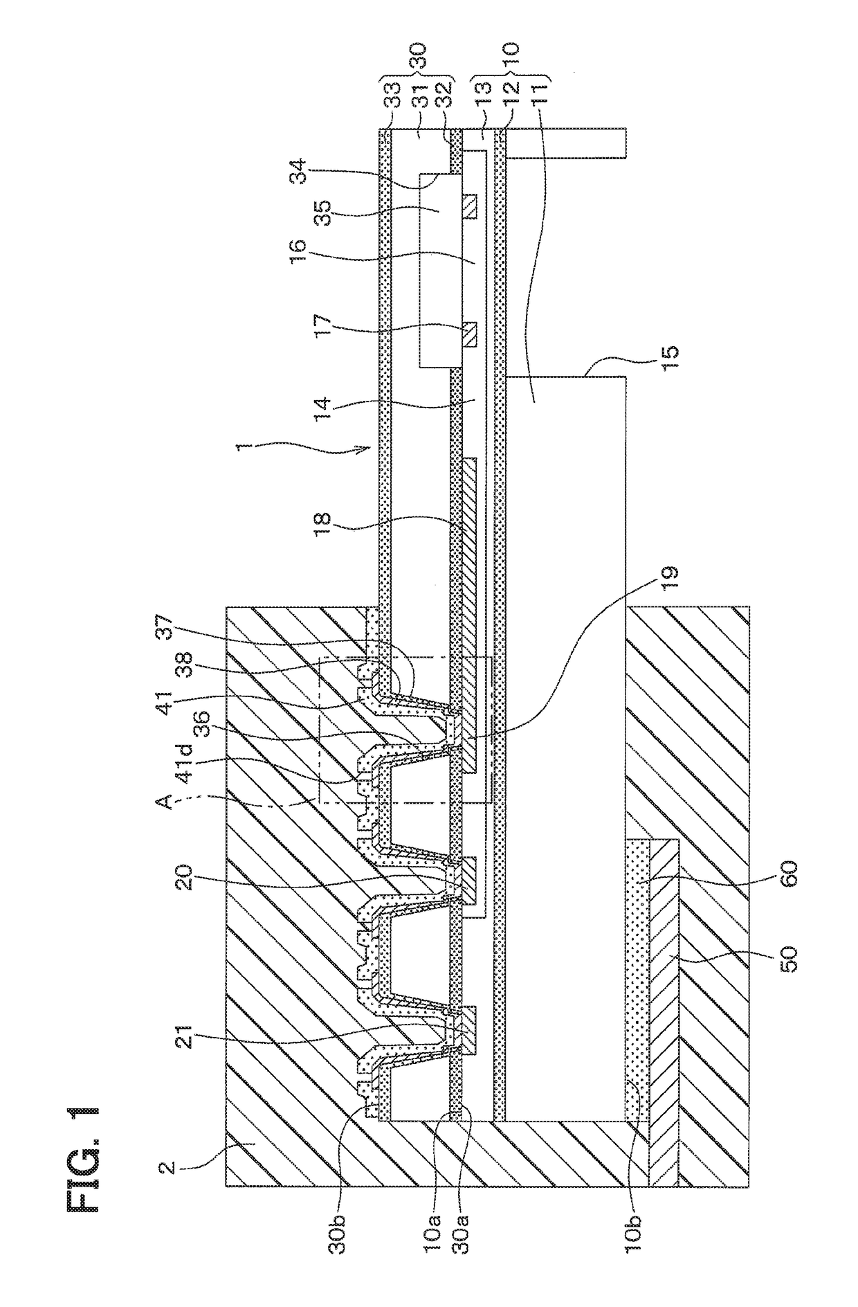
[0020]A first embodiment is described in the following with reference to the drawings. The present embodiment describes an example in which a semiconductor device is applied to a pressure sensor. It is noted that the pressure sensor as the semiconductor may be, for example, mounted on an automobile to detect the pressure of gas emitted from an oil pump.
[0021]As illustrated in FIG. 1, the semiconductor device includes a sensor 1 and a molded resign 2 which seals one part of the sensor 1 for support. First of all, the configuration of the sensor 1 according to the present embodiment 1 is described in the following.
[0022]The sensor 1 includes a sensor substrate 10 that has a first surface 10aand a second surface 10b at a side opposite to the first surface 10a. In the present embodiment, a support substrate 11, an insulation film 12 and a semiconductor layer 13 are stacked in order, and configured by an SOI (Silicon on
[0023]Insulator) substrate having a rectangular shape in a plan view ...
second embodiment
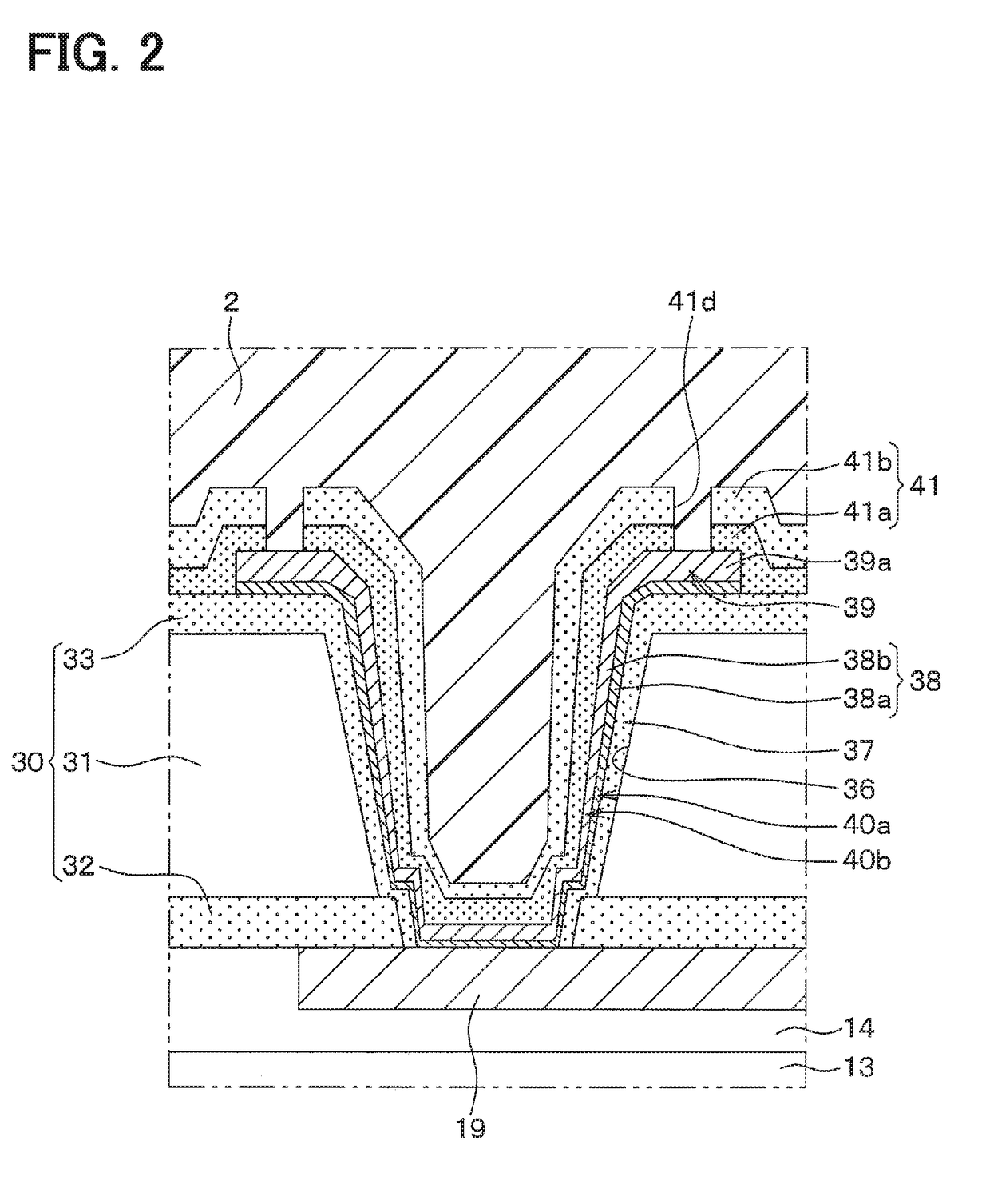
[0066]A second embodiment is described herein. The present embodiment describes the modification of a location where the slit 41d is formed. Other than that, the second embodiment is similar to the first embodiment. Therefore, the description of the common parts in the first and second embodiments is omitted.
[0067]In this embodiment, as illustrated in FIGS. 7 and 8, the slit 41d is formed at the protective film 41 to surround the wiring layer 39 viewed in a normal direction with respect to the first surface 10a of the sensor substrate 10. In the present embodiment, the lower protective film 41a and the insulation film 33 are configured by TEOS as the same material. In a situation where the crack occurs at the lower protective film 41a, the crack might be conducted to the insulation film 33. Accordingly, the slit 41d is formed to penetrate the lower protective film 41a and the insulation film 33 to reach the substrate 31. In other words, the slit 41d is formed to expose the substrate...
third embodiment
[0071]A third embodiment is described in the following. The present embodiment refers to the modification of the protective film 41. Other than that, the third embodiment is similar to the first embodiment. Therefore, the description of the common parts in the first and third embodiments is omitted.
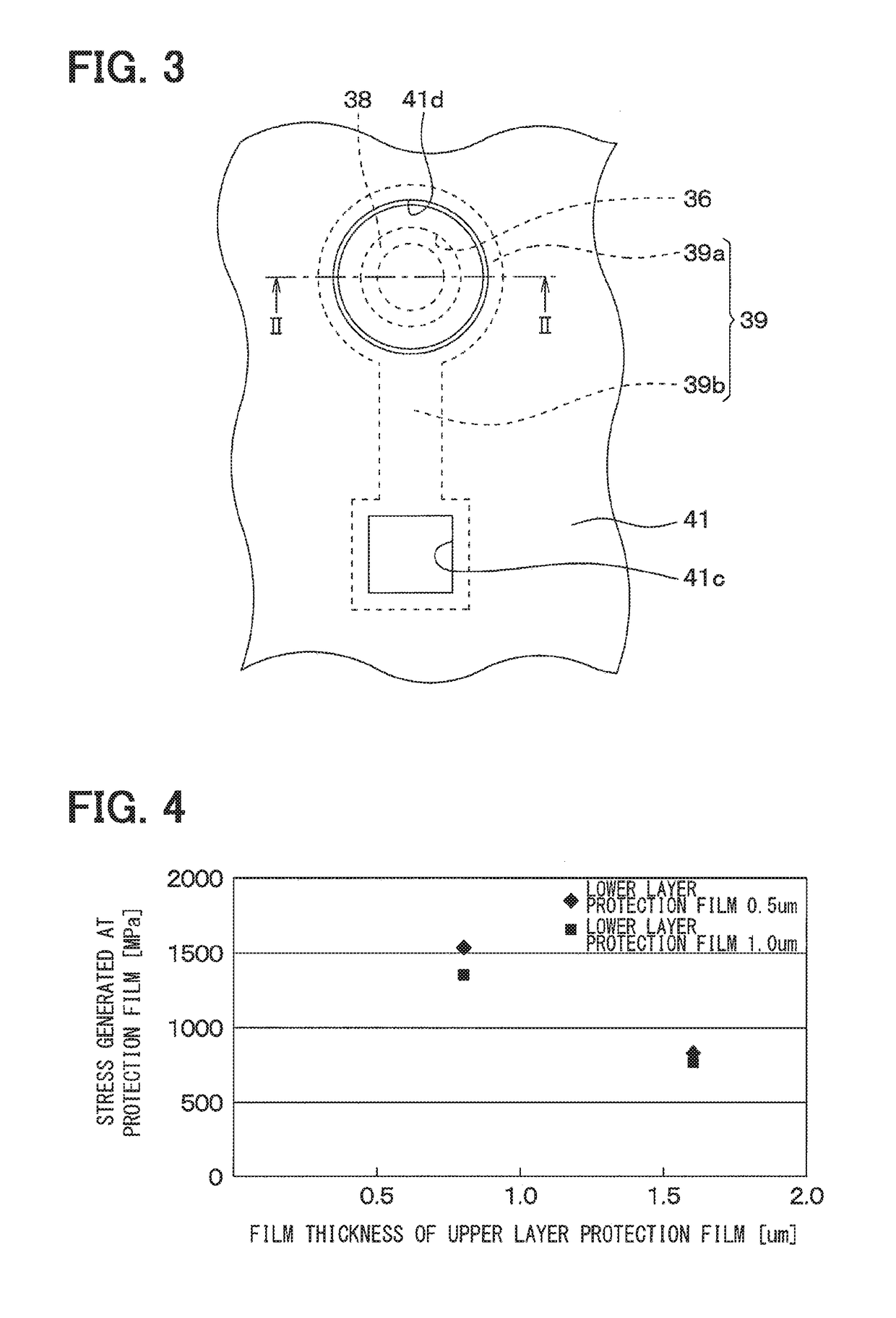
[0072]In the present embodiment, as illustrated in FIG. 9, the protective film 41 is not arranged on the wall surface of the through-hole 36. That is, it is configured such that the protective film 41 is not arranged at the location where the stress is concentrated, in other words, the location where the crack easily occurs. It is noted that FIG. 9 corresponds to an enlarged view of the region A illustrated in FIG. 1.
[0073]Accordingly, the occurrence of cracks on the protective film is reduced by not providing the protective film 41 at the location where the stress is concentrated.
Other Embodiments
[0074]While the present disclosure has been described with reference to embodiments thereof,...
PUM
Abstract
A semiconductor device includes: a first substrate having connection parts at a first surface; a second substrate bonded with the first substrate having through-holes in a stacking direction of the first and second substrates for respectively exposing the connection parts; through-electrodes respectively arranged at through-holes and electrically connected with the connection parts; and a protective film for integrally covering the through-electrodes. Frame-shaped slits are formed to respectively surround the through-holes when viewed in a normal direction with respect to the first surface of the first substrate. The protective film is separated by the slit into a region inside the slit and a region outside the slit.
Description
CROSS REFERENCE TO RELATED APPLICATION[0001]This application is based on Japanese Patent Application No. 2016-41427 filed on Mar. 3, 2016, the disclosure of which is incorporated herein by reference.TECHNICAL FIELD[0002]The present disclosure relates to a semiconductor device. The semiconductor device has a first substrate and a second substrate. Both of the first and second substrates are joined together. A through-electrode, which is electrically connected with a connection part formed at the first substrate, is formed at the second substrate.BACKGROUND ART[0003]It has been known that a pressure sensor, which is configured by having a first substrate and a second substrate, has been introduced in, for example, Patent Literature 1. In particular, with regard to this semiconductor device, the first substrate includes one surface having a gauge resistor and a plurality of connection parts, which are electrically connected with the gauge resistor, and having a concave part, which thin...
Claims
Application Information
Patent Timeline
Application Date:The date an application was filed.
Publication Date:The date a patent or application was officially published.
First Publication Date:The earliest publication date of a patent with the same application number.
Issue Date:Publication date of the patent grant document.
PCT Entry Date:The Entry date of PCT National Phase.
Estimated Expiry Date:The statutory expiry date of a patent right according to the Patent Law, and it is the longest term of protection that the patent right can achieve without the termination of the patent right due to other reasons(Term extension factor has been taken into account ).
Invalid Date:Actual expiry date is based on effective date or publication date of legal transaction data of invalid patent.

