

Through electrode substrate and manufacturing method thereof
a technology of through electrodes and substrates, which is applied in the direction of printed circuit manufacturing, printed circuit aspects, printed element electric connection formation, etc., can solve the problems of warpage and/or distortion of substrates, uneven layout of holes non-uniform hole distribution density in through electrode substrates, etc., to inhibit warpage and/or distortion.
- Summary
- Abstract
- Description
- Claims
- Application Information
AI Technical Summary
Benefits of technology
Problems solved by technology
Method used
Image

Examples
first embodiment
[0061]A first embodiment is described with reference to FIGS. 1 to 3G.
[0062]Through Electrode Substrate
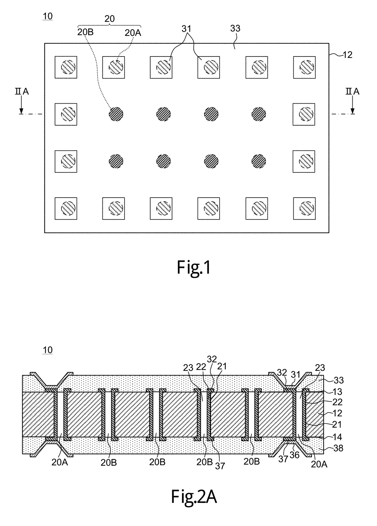
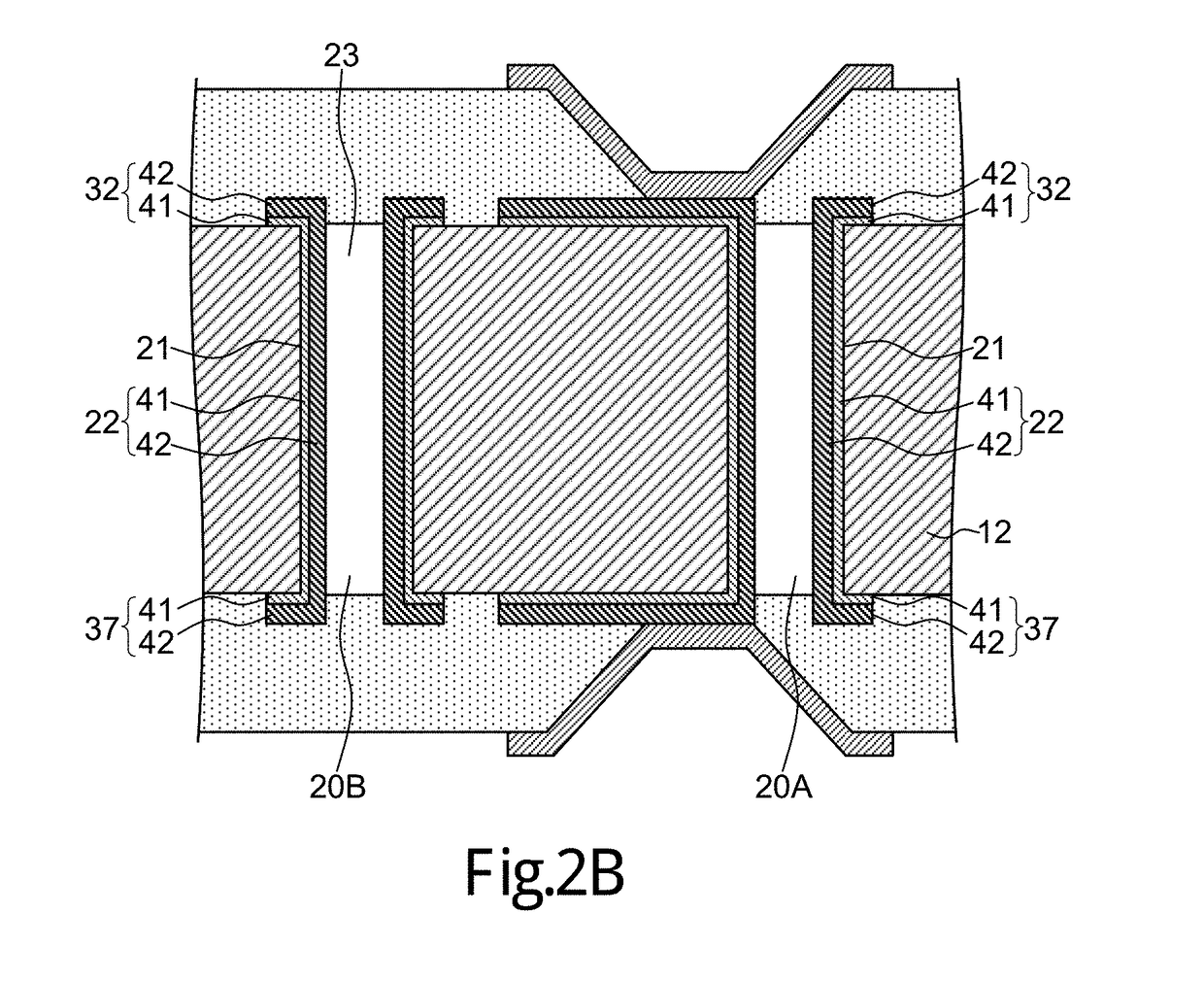
[0063]Firstly, a through electrode substrate 10 according to the embodiment is described with reference to FIGS. 1 and 2A. FIG. 1 is a plan view showing the through electrode substrate 10. FIG. 2A is a sectional view of the through electrode substrate 10 of FIG. 1 cut along one-dot chain lines, which is seen from a IIA-IIA direction.
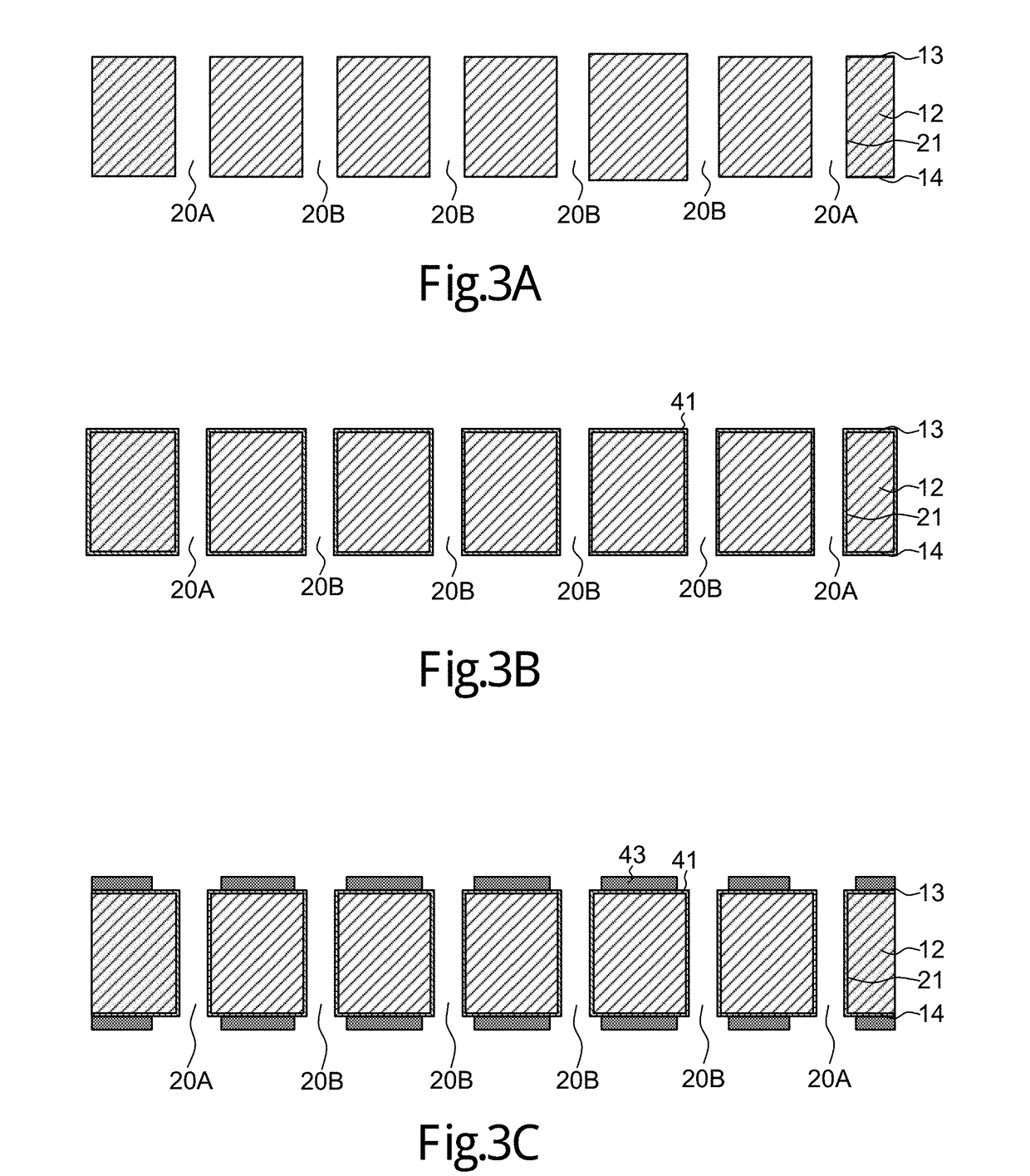
[0064]The through electrode substrate 10 comprises a substrate 12, a plurality of holes provided in the substrate 12, and hole electrode parts 22 provided inside the holes. As described later, the holes at least include two types of holes of a first hole 20A and a second hole 20B. In the below description, when structures applicable both to the first hole 20A and the second hole 20B, the first hole 20A and the second hole 20B are referred to as holes 20 as a general term.
[0065]In addition, the through electrode substrate 10 further comprises a first ele...
first modification example
[0114]The above embodiment shows the example in which both the first hole 20A and the second hole 20B are through holes which pass through the substrate 12 from the first surface 13 side to the second surface 14 side. However, not limited thereto, the second hole 20B may be a non-through hole that does not pass through the substrate 12. For example, as shown in FIG. 4A, the second hole 20B may be a non-through hole that is formed not to reach the second surface 14 of the substrate 12. Alternatively, as shown in FIG. 4B, the second hole 20B may be a non-through hole that is formed not to reach the first surface 13 of the substrate 12. When the first hole 20B is a non-through hole, the second hole 20B includes a sidewall 21 and a bottom 24. The hole electrode part 22 is provided on the sidewall 21 and on the bottom 24.
[0115]Even when the second holes 20B are non-through holes, the distribution density of the holes 20A, 20B can be made more uniform by providing the second holes 20B in ...
second modification example
[0116]The above embodiment shows the example in which the the wiring 32, 37 having the same layer structure as that of the hole electrode part 22 is simultaneously formed with the hole electrode part 22. However, not limited thereto, the wiring 32, 37 having a structure different from that of the hole electrode part 22 may be formed at a different timing from that of the hole electrode part 22. Herebelow, a manufacturing method of the through electrode substrate 10 in this modification example is described with reference to FIG. 5A through 5D.
[0117]Firstly, similarly to the above embodiment, the seed layer 41 and the plating layer 42 are formed on the holes 20A and 20B of the substrate 12 to obtain the aforementioned intermediate product shown in FIG. 3E. Then, as shown in FIG. 5A, a portion of the seed layer 41 and the plating layer 42, which is present on the first surface 13 and the second surface 14 of the substrate 12, is removed. For example, a chemical mechanical grinding met...
PUM
 Abstract
Description
Claims
Application Information