
Antenna module

a technology of antenna modules and circuit layers, applied in the field of antenna modules, can solve the problems of disadvantageous generation of dead space in one of the antenna and circuit layers, and achieve the effect of improving the efficiency of the circuit layer

Active Publication Date: 2019-03-21
TDK CORPARATION
View PDF7 Cites 4 Cited by
  • Summary
  • Abstract
  • Description
  • Claims
  • Application Information

AI Technical Summary

Benefits of technology

The present invention aims to improve the use of the circuit layer in an antenna module. This is achieved by stacking the antenna layer and circuit layer one over the other, which helps to increase efficiency in utilizing the circuit layer.

Problems solved by technology

However, a planar size that the antenna layer requires and a planar size that the circuit layer requires do not necessarily coincide with each other, so that when the antenna layer and the circuit layer are stacked one over the other, a dead space may be disadvantageously generated in one of the antenna and circuit layers.

Method used


Image

  • Antenna module
  • Antenna module
  • Antenna module

Examples


first embodiment

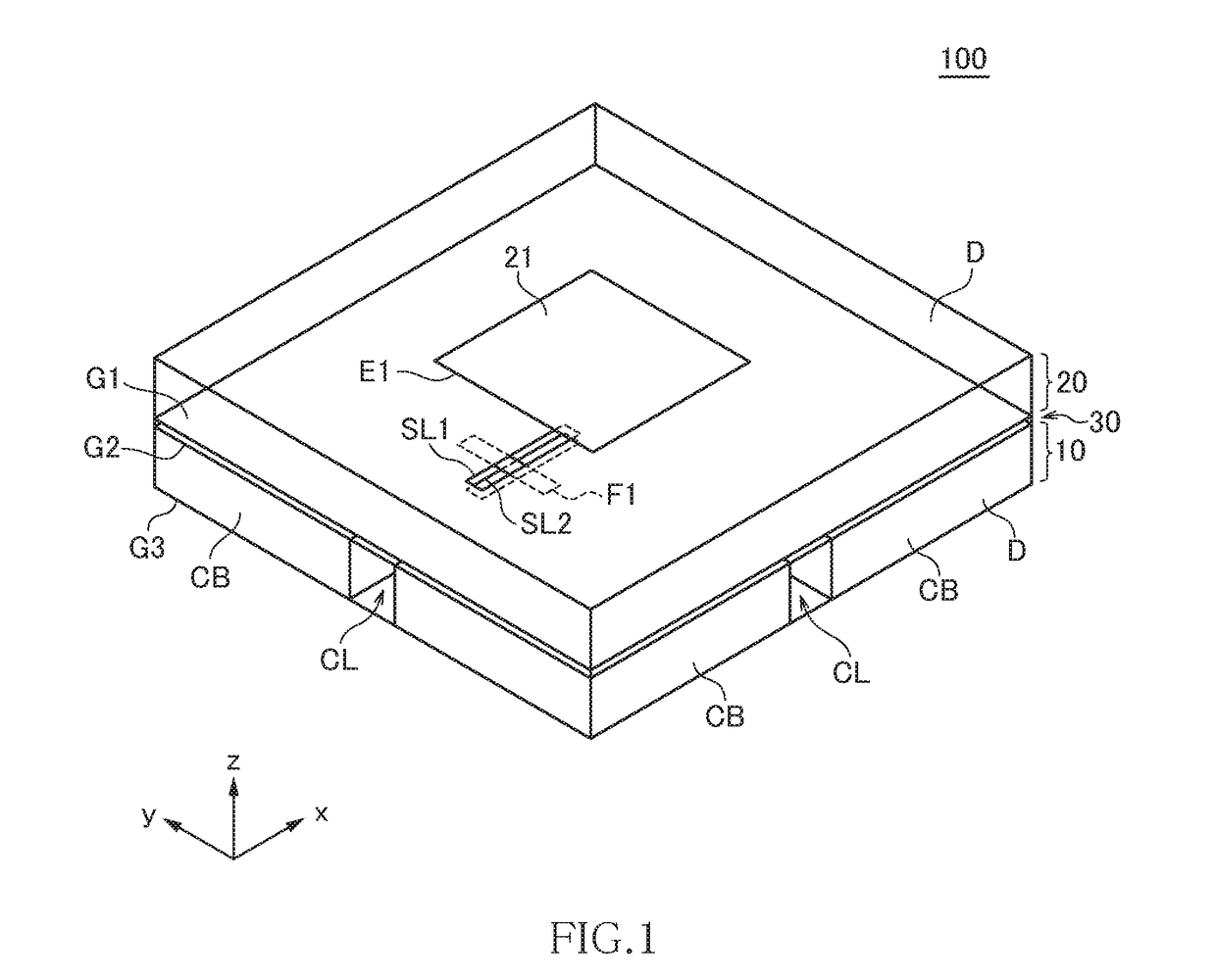
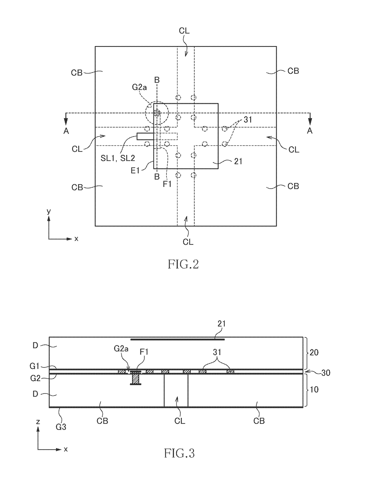
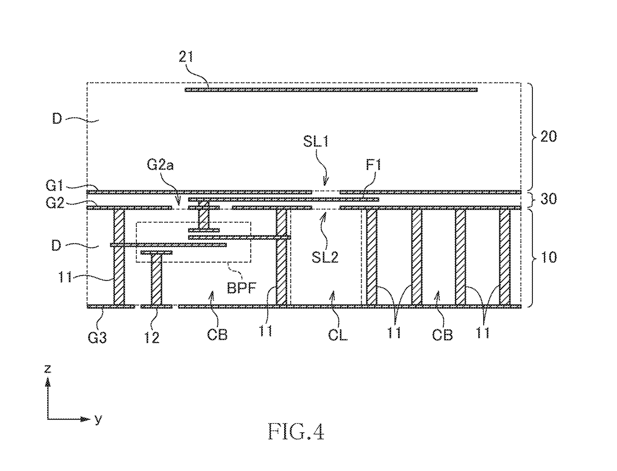
[0040]FIG. 1 is a transparent perspective view schematically illustrating an antenna module 100 according to the first embodiment of the present invention. FIG. 2 is a transparent plan view schematically illustrating the antenna module 100, FIG. 3 is a schematic cross-sectional view of the antenna module 100 taken along line A-A of FIG. 2, and FIG. 4 is a schematic cross-sectional view of an end face taken along line B-B of FIG. 2.

[0041]The antenna module 100 according to the present embodiment is a module that performs wireless communication using a millimeter wave band and, as illustrated in FIGS. 1 to 4, has a circuit layer 10 as a lower layer, an antenna layer 20 as an upper layer, and a feed layer 30 positioned between the circuit layer 10 and the antenna layer 20. The circuit layer 10, antenna layer 20, and feed layer 30 each have a configuration in which various conductor patterns are formed on the inside of or on the surface of a dielectric layer D. Although not particularly...

second embodiment

[0052]FIG. 6 is a transparent plan view schematically illustrating an antenna module 200 according to the second embodiment of the present invention.FIG. 7 is a schematic cross-sectional view of an end face taken along line C-C of FIG. 6.

[0053]As illustrated in FIGS. 6 and 7, the antenna module 200 according to the second embodiment differs from the antenna module 100 according to the first embodiment in that the circuit layer 10 additionally includes a coupler pattern C1 and an external terminal 13 connected to the coupler pattern C1. Other configurations are basically the same as those of the antenna module 100 according to the first embodiment, so the same reference numerals are given to the same elements, and overlapping description will be omitted.

[0054]The coupler pattern C1 is a band-like conductor pattern extending in the y-direction and is disposed at a position overlapping the feed pattern F1 through the slot SL2. With this configuration, the feed pattern F1 and the couple...

third embodiment

[0056]FIG. 8 is a transparent perspective view schematically illustrating an antenna module 300 according to the third embodiment of the present invention. FIG. 9 is a transparent plan view schematically illustrating the antenna module 300, and FIG. 10 is a schematic cross-sectional view of an end face taken along line D-D of FIG. 9.

[0057]As illustrated in FIGS. 8 to 10, the antenna module 300 according to the third embodiment differs from the antenna module 100 according to the first embodiment in that slots SL3 and SL4 are additionally formed in the ground patterns G1 and G2, respectively, and that a coupler pattern C2 is provided at a position overlapping the slots SL3 and SL4. Other configurations are basically the same as those of the antenna module 100 according to the first embodiment, so the same reference numerals are given to the same elements, and overlapping description will be omitted.

[0058]The slots SL3 and SL4 each have a shape elongated in the x-direction. The slots ...


PUM


Abstract

Disclosed herein is an antenna device that includes a circuit layer having a filter circuit, an antenna layer stacked on the circuit layer and having a radiation conductor, a feed layer positioned between the circuit layer and the antenna layer and having a first feed pattern connected to the filter circuit and electromagnetically coupled to the radiation conductor, a first ground pattern provided between the antenna layer and the feed layer, and a second ground pattern provided between the circuit layer and the feed layer. The first and second ground patterns have first and second slots, respectively, at least partially overlapping each other as viewed in a stacking direction. The first feed pattern at least partially overlaps the radiation conductor and the first and second slots.

Description

BACKGROUND OF THE INVENTIONField of the Invention[0001]The present invention relates to an antenna module and, more particularly, to an antenna module in which an antenna layer including a radiation conductor and a circuit layer including a filter circuit are integrated.Description of Related Art[0002]As the antenna module in which an antenna layer including a radiation conductor and a circuit layer including a filter circuit are integrated, the antenna module described in JP 2004-040597 A is known. In the antenna module described in JP 2004-040597 A, the antenna layer and the circuit layer are staked one over the other with a ground pattern interposed therebetween, thereby preventing mutual interference between the antenna layer and the circuit layer.[0003]However, a planar size that the antenna layer requires and a planar size that the circuit layer requires do not necessarily coincide with each other, so that when the antenna layer and the circuit layer are stacked one over the o...

Claims


Application Information

Patent Timeline
Patent Type & Authority Applications(United States)
IPC IPC(8): H01Q9/04H01Q1/48H01Q21/06
CPCH01Q9/0457H01Q1/48H01Q21/061H01Q1/38H01Q1/50H01Q21/0006H01Q23/00H01P5/187H01Q3/267H01Q9/0414H01Q9/0435H01Q21/065H01Q21/24
Inventor HARA, YASUYUKISOTOMA, NAOKI
Owner TDK CORPARATION
Learn More