Photocatalyst electrode, artificial photosynthesis module, and artificial photosynthesis device

a photocatalyst and electrode technology, applied in the direction of electrolysis components, electrode coatings, multiple component coatings, etc., can solve the problems of increasing the electrical resistance of the conductive part, adverse effects, and difficulty in obtaining effects, so as to improve the creation efficiency and reduce the electric resistance

Active Publication Date: 2019-04-18
FUJIFILM CORP +1
View PDF0 Cites 4 Cited by
  • Summary
  • Abstract
  • Description
  • Claims
  • Application Information

AI Technical Summary

Benefits of technology

[0030]According to the invention, even in a case where the transparent conductive laye...

Problems solved by technology

However, it is necessary to form the electrode through a solution process or the like in making the electrode, the shape of the surface of the electrode is turned into a rough shape under the influence of dryness or the like, contact resistance is generated at an interface between the electrode and the transparent electrode, and the effect is not ...

Method used


Image

  • Photocatalyst electrode, artificial photosynthesis module, and artificial photosynthesis device
  • Photocatalyst electrode, artificial photosynthesis module, and artificial photosynthesis device
  • Photocatalyst electrode, artificial photosynthesis module, and artificial photosynthesis device

Examples


example 1

[0217]

[0218]A glass substrate on which an indium tin oxide (ITO) film was formed was prepared. The glass substrate is 10 cm×11 cm in sizes. A BiOI precursor was formed in a region of 10 cm×10 cm by the electrodeposition method, leaving a 1-cm portion on the glass substrate. Thereafter, a dimethyl sulfoxide solution (DMSO solution) in which VO(acac)2(vanadyl acetylacetonate) was dissolved was added dropwise and baked, and a BiVO4 substrate was formed.

[0219]

[0220]The BiVO4 substrate made as described above was immersed in an electrolytic solution in which iron ions and nickel ions were dissolved, and a co-catalyst was modified using light of air mass (AM) 1.5 G by a photo electrodeposition method.

[0221]

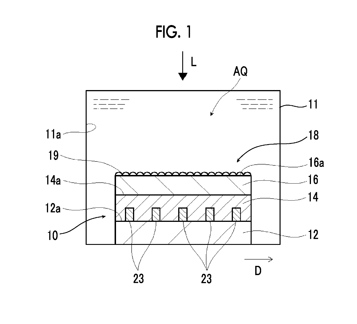
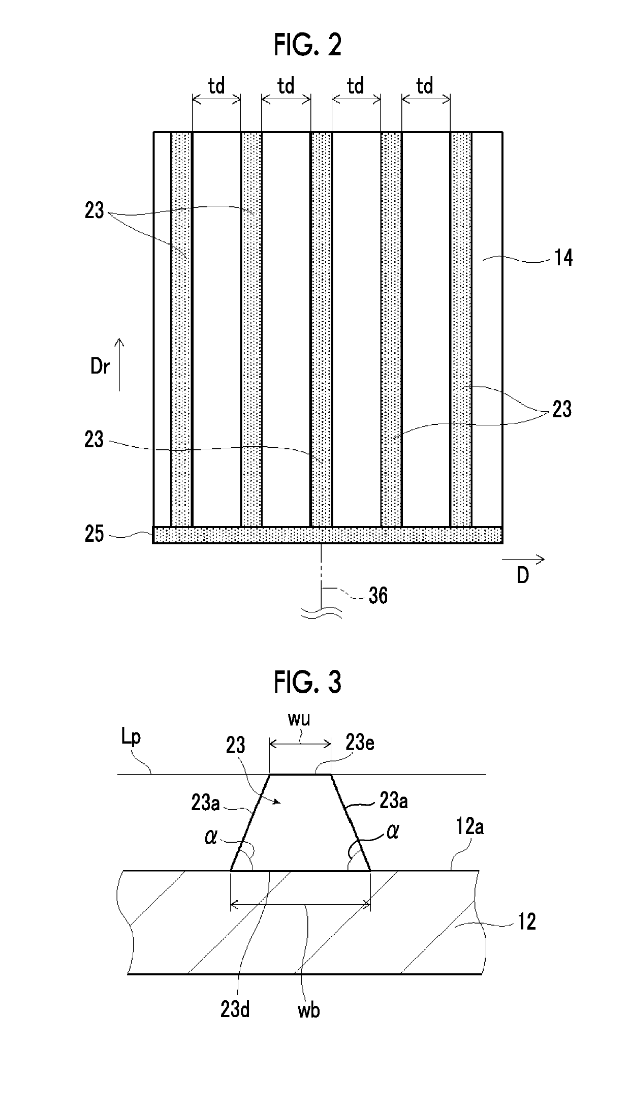
[0222]A plurality of copper wires having a width of 0.1 mm were formed at width intervals of 20 mm on the formed BiVO4 substrate of 10 cm×10 cm, linear metal electrical conductors were obtained, and the linear metal electrical conductors were protected with an epoxy adhesive. An ITO mem...

example 2

[0227]A plurality of copper wires having a width of 0.1 mm were formed at intervals of 20 mm on a glass substrate of 10 cm×11 cm. Thereafter, an ITO film that coats the copper wires is formed on the glass substrate. Accordingly, an ITO substrate was obtained on which a conductive layer having linear metal electrical conductors obtained by the copper wires being disposed at intervals of 20 mm was formed. A BiOI precursor was formed in a region of 10 cm×10 cm by the electrodeposition method, leaving a 1-cm portion on the ITO substrate of 10 cm×11 cm. Thereafter, a dimethyl sulfoxide solution (DMSO solution) in which VO(acac)2(vanadyl acetylacetonate) was dissolved was added dropwise and baked, and a BiVO4 substrate was formed. Thereafter, the co-catalyst modification was performed by the same method as that of Example 1, an ITO membrane portion of the formed BiVO4 substrate of 10 cm×10 cm was fixed with a clip, and a photoelectrochemical measurement was carried out.

[0228]Additionally,...

example 3

[0229]A plurality of copper wires having a width of 0.1 mm were formed at intervals of 20 mm on a glass substrate of 10 cm×11 cm. Thereafter, the copper wires were processed using the photolithography. Thereafter, an ITO film that coats the copper wires is formed on the glass substrate. Since the subsequent manufacturing process and the photoelectrochemical measuring method are the same as those of Example 2, the detailed description thereof will be omitted.

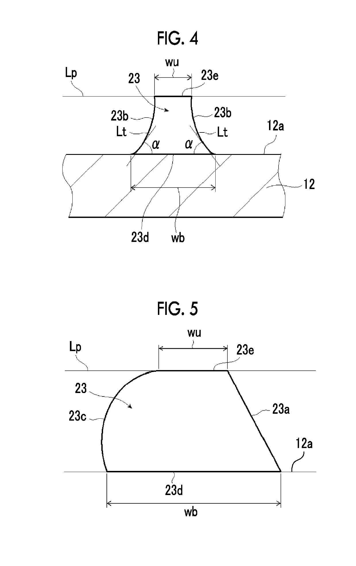
[0230]Regarding Example 3, the taper angle was 60° in a case where a cross-section of the copper wires was observed using the scanning electron microscope.

[0231]Additionally, also in Example 3, a small-sized BiVO4 substrate as described above was obtained similarly to Example 1. Then, the co-catalyst modification was applied as described above, and a photoelectrochemical measurement was carried out on the small-sized BiVO4 substrate.


PUM


Abstract

Provided are a photocatalyst electrode, an artificial photosynthesis module, and an artificial photosynthesis device that have low electrical resistance, even in a case where the area is increased, in a case where a transparent conductive layer is used. The photocatalyst electrode is a photocatalyst electrode that has a substrate, a transparent conductive layer, a photocatalyst layer, and a linear metal electrical conductor, and splits water with light to produce a gas. The substrate, the transparent conductive layer, and the photocatalyst layer are laminated in this order, and the linear metal electrical conductor is in contact with the transparent conductive layer. The artificial photosynthesis module has the oxygen evolution electrode that splits the water with the light to produce oxygen, and a hydrogen evolution electrode that splits the water with the light to produce hydrogen. The oxygen evolution electrode and the hydrogen evolution electrode are disposed in series in a traveling direction of the light. At least one of the oxygen evolution electrode or the hydrogen evolution electrode has the configuration of the above-described photocatalyst electrode. The artificial photosynthesis device has the artificial photosynthesis module, and circulates and utilizes water.

Description

CROSS-REFERENCE TO RELATED APPLICATIONS[0001]This application is a Continuation of PCT International Application No. PCT / JP2017 / 017414 filed on May 8, 2017, which claims priority under 35 U.S.C. § 119(a) to Japanese Patent Application No. 2016-113743 filed on Jun. 7, 2016. The above application is hereby expressly incorporated by reference, in its entirety, into the present application.BACKGROUND OF THE INVENTION1. Field of the Invention[0002]The present invention relates to a photocatalyst electrode, an artificial photosynthesis module, and an artificial photosynthesis device that split water with light to produce gas, and particularly, to a photocatalyst electrode, an artificial photosynthesis module, and an artificial photosynthesis device that use a transparent conductive layer.2. Description of the Related Art[0003]Nowadays, water is splitted using a photocatalyst and utilizing solar light energy, which is renewable energy, to obtain gases, such as hydrogen gas and oxygen gas.[...

Claims


Application Information

Patent Timeline
IPC IPC(8): C25B11/04C25B1/04C25B1/00C25B9/06C25B9/17
CPCC25B11/0478C25B1/04C25B1/003C25B9/06C25B11/0405Y02E60/36C25B1/55C25B9/65C25B9/17C25B11/051C25B11/091
Inventor ABURAYA, YOSHIHIROTSUKAHARA, JIROYOSHIDA, SATOSHINAGATE, HIROSHIKOBAYASHI, HIROYUKI
Owner FUJIFILM CORP
Why Eureka
Try Eureka