Method and device for severing a microchip from a wafer and arranging the microchip on a substrate

Active Publication Date: 2019-04-25
JENOPTIK OPTICAL SYST
View PDF0 Cites 0 Cited by
  • Summary
  • Abstract
  • Description
  • Claims
  • Application Information

AI Technical Summary

Benefits of technology

[0018]It is the object of the invention to provide a device which can be produced more economically

Problems solved by technology

The small thickness and small surface area result in specific problems with regard to handling, precise positioning, planarity, stable connection and, as the case may be, conductive bonding of the microchip.
Microchips having such small geometric dimensions cannot be processed through conventional automatic populating devices, glue/solder connections, wire bonding or flip chip bonding.
For example, while there are micro-manipulators for manipulating samples of focused ion beam (FIB) sections, they are very expensive to use and are not suitable for a

Method used


Image

  • Method and device for severing a microchip from a wafer and arranging the microchip on a substrate
  • Method and device for severing a microchip from a wafer and arranging the microchip on a substrate
  • Method and device for severing a microchip from a wafer and arranging the microchip on a substrate

Examples


Example

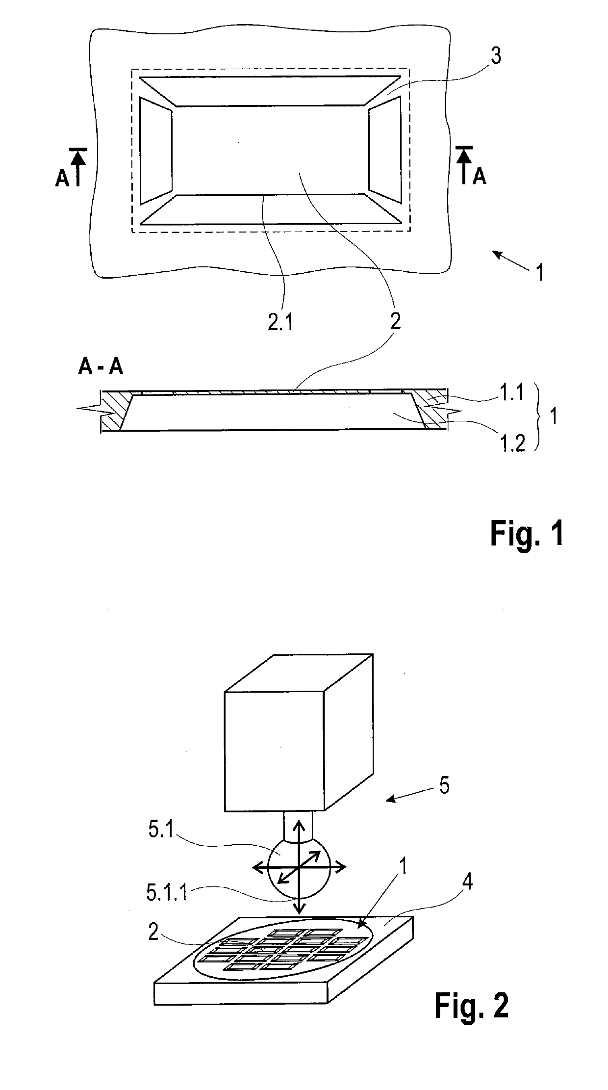
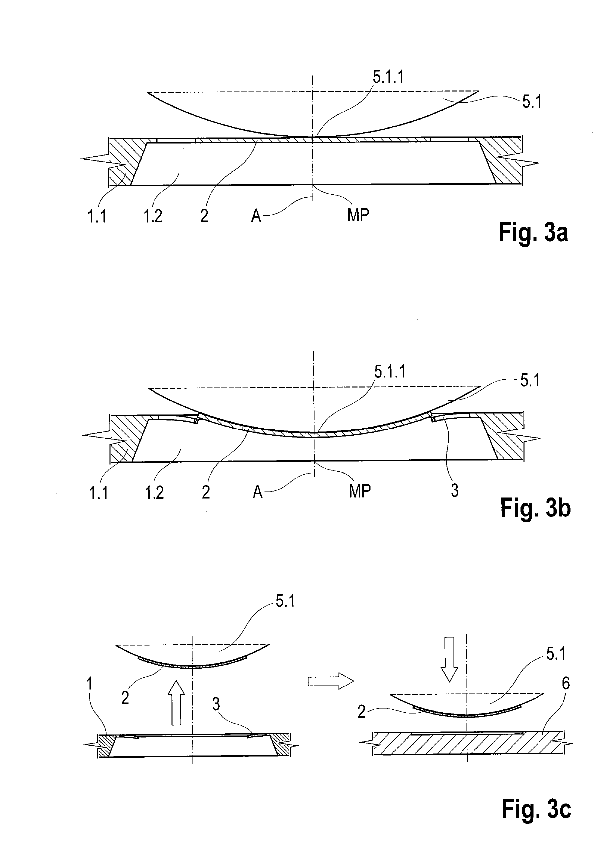
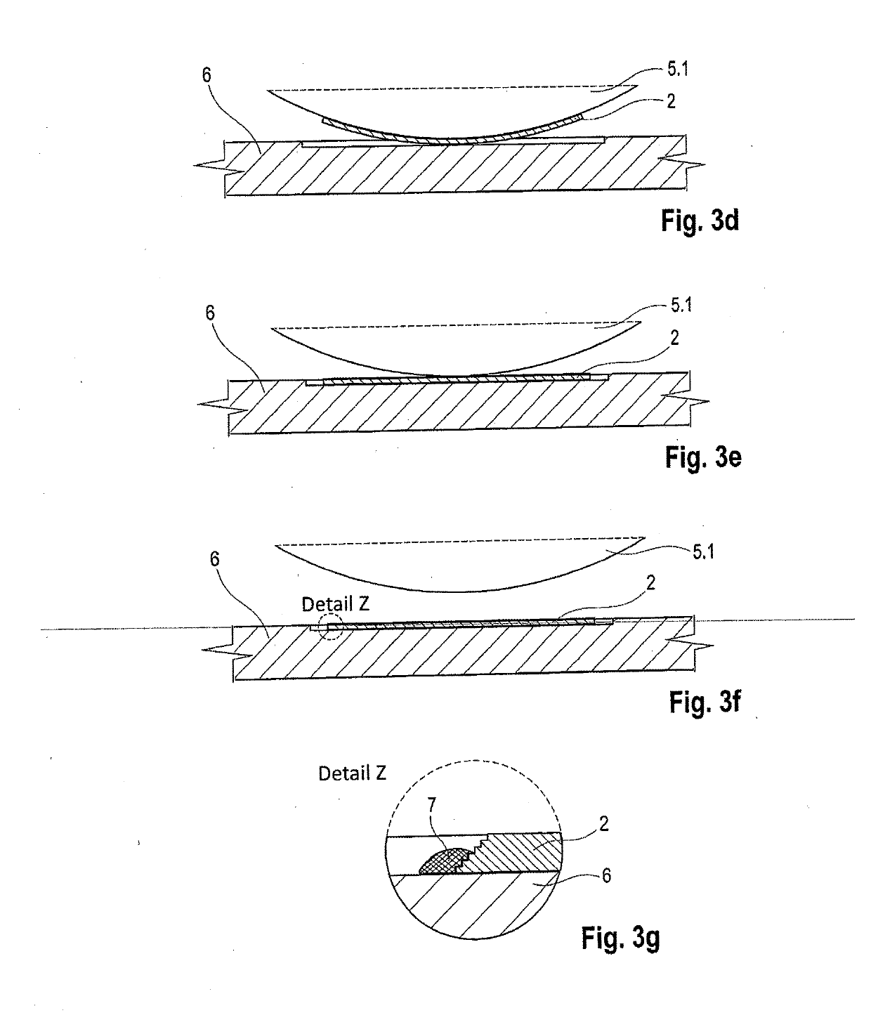
[0025]The device serves for separating microchips 2 from a wafer 1, particularly microchips 2 with the dimensions of a membrane chip. The wafer 1 is formed by a carrier body 1.1 with cutouts 1.2 in which one of the microchips 2 is held in each instance via retaining tabs 3. A wafer 1 of this type is shown schematically in FIG. 1. The microchips 2 have very small dimensions, e.g., 3 μm×100 μm×250 μm, and therefore have a very small thickness. Usually, the most common shape of the circumferential edge 2.1 of the microchip 2 is a rectangle. Other circumferential shapes such as circles or triangles are conceivable. In this regard, it is advantageous for a method according to the invention when the retaining tabs 3 engage at the microchip 2 so as to be equidistant from the center point of the microchip 2 and are preferably arranged at corners possibly formed by the circumferential edge 2.1 so as to be uniformly distributed around the circumferential edge 2.1. The retaining tabs 3 can be ...


PUM


Abstract

Method and device for severing a microchip from a wafer and arranging the microchip on a substrate, wherein the microchip is contact-bonded to the free end of a tip during severing and accordingly adheres to the tip through adhesive force while the substrate is transported. A coordinate measuring machine can advantageously be used as device.

Description

RELATED APPLICATIONS[0001]The present application is a U.S. National Stage application of International PCT Application No. PCT / DE2017 / 100035 filed on Jan. 23, 2017 which claims priority benefit of German Application No. DE 10 2016 001 322.2 filed on Jan. 29, 2016, the contents of each are incorporated by reference in their entirety.BACKGROUND OF THE INVENTION[0002]As more and more component assemblies and / or component parts become progressively more complex in increasingly smaller units, e.g., in semiconductor engineering, microsystems technology, telecommunications, security technology, energy production or measuring technology, the component assemblies and / or component parts are increasingly embodied by individual chips which are arranged adjacent to one another on a substrate.[0003]Chips of this kind can have outer dimensions in the micrometer range.[0004]Within the meaning of the present description, “substrate” designates a base material serving as a carrier for, e.g., printed...

Claims


Application Information

Patent Timeline
IPC IPC(8): H01L21/67H01L23/00H01L21/683B65G47/92
CPCH01L21/67144H01L24/97H01L21/67132H01L21/6831B65G47/92H01L21/78H01L2221/68363H01L24/799H01L24/98H01L2224/7999H01L2224/98
Inventor PANITZ, MEIK
Owner JENOPTIK OPTICAL SYST
Why Eureka
Try Eureka