Power conversion apparatus

a power conversion apparatus and power conversion technology, applied in the direction of control systems, solid-state devices, basic electric elements, etc., can solve the problems of low current amount, low efficiency, and high current amount of control electrodes, so as to reduce voltage variation, reduce voltage variation, and reduce the effect of voltage variation

Active Publication Date: 2019-04-25
DENSO CORP
View PDF2 Cites 3 Cited by
  • Summary
  • Abstract
  • Description
  • Claims
  • Application Information

AI Technical Summary

Benefits of technology

[0010]The present disclosure is directed to providing a power conversion apparatus which can cause a plurality of semiconductor elements to perform switching at the same time and which can reduce variation in voltages applied to control electrodes of the individual semiconductor elements.
[0013]It is therefore possible to reduce variation in voltages applied to the control electrodes of the individual semiconductor elements. That is, as described above, if the plurality of semiconductor elements connected in parallel to each other are caused to perform switching at the same time, reference potentials of the individual semiconductor elements are likely to vary. As a result, it may occur that a current flows from a semiconductor element with a higher reference potential to a semiconductor element with a lower reference potential via the reference wiring. However, in the present aspect, because the parasitic inductance in the reference wiring is made smaller, it is possible to make induced electromotive force ΔV which occurs at the reference wiring when a current flows smaller. As described above, while VG+ΔV is applied to a control electrode of a semiconductor element with a lower reference potential, and VG−ΔV is applied to a semiconductor element with a higher reference potential, because it is possible to make ΔV smaller in the present aspect, it is possible to suppress variation in voltages applied to the control electrodes of the respective semiconductor elements. Therefore, it is possible to suppress defects such as degradation of semiconductor elements as a result of an excessively high voltage being applied to a control electrode of the semiconductor element with a lower reference potential and failure of semiconductor elements to be correctly turned on as a result of only a low voltage being applied to a control electrode of the semiconductor element with a higher reference potential.
[0014]As described above, according to the present aspect, it is possible to provide a power conversion apparatus which can cause a plurality of semiconductor elements to perform switching at the same time and which can reduce variation in voltages applied to control electrodes of individual semiconductor elements.

Problems solved by technology

However, if a plurality of semiconductor elements are caused to perform switching at the same time, voltages applied to control electrodes of the semiconductor elements are likely to vary.
Therefore, because a voltage higher than a normal control voltage VG is applied to the control electrode, there can be a possibility that this semiconductor element may degrade.
Therefore, this semiconductor element is not correctly turned on, and a current amount is likely to decrease.

Method used


Image

  • Power conversion apparatus
  • Power conversion apparatus
  • Power conversion apparatus

Examples


fourth embodiment

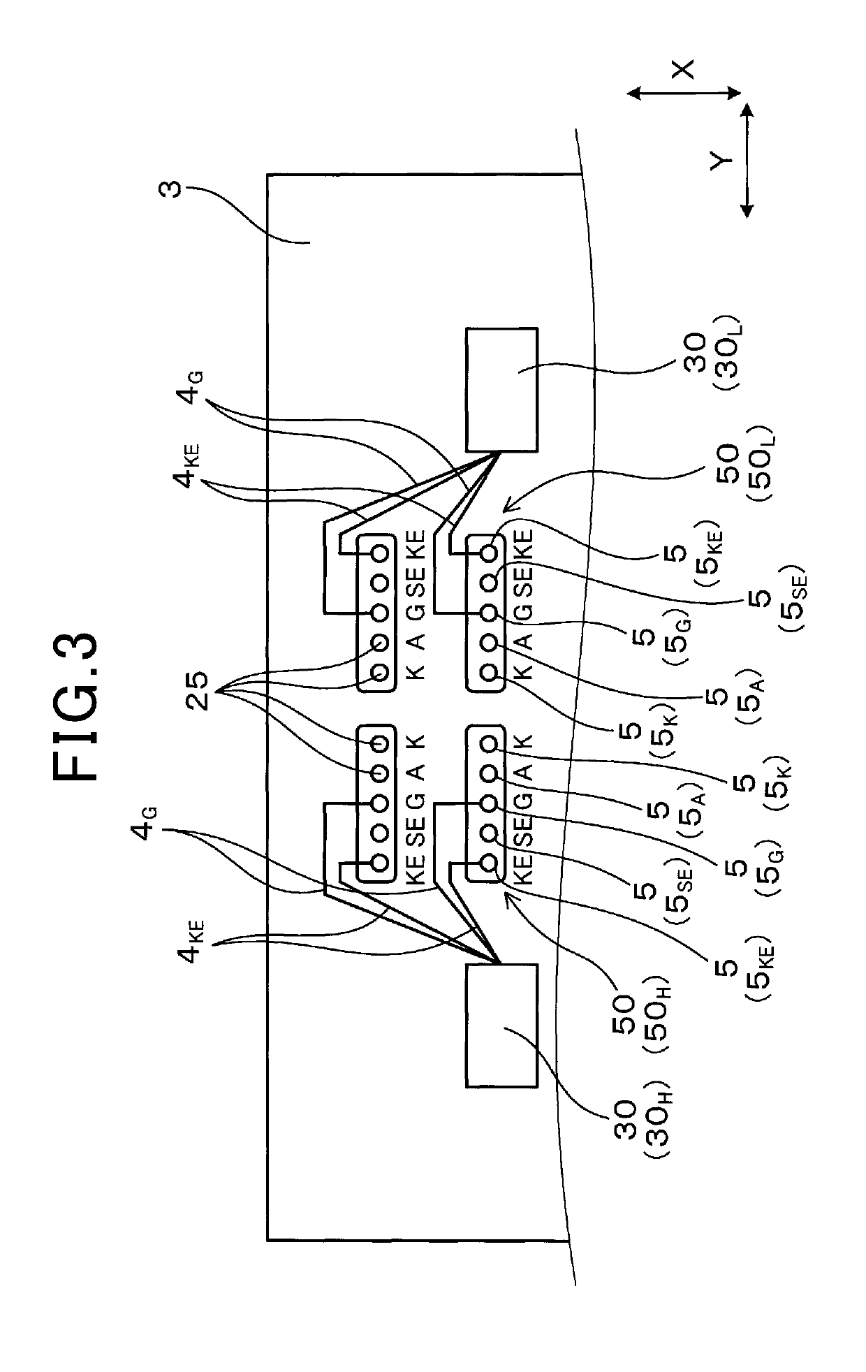
[0098]The present embodiment is an example in which the configuration of the control circuit unit 3 is changed. As illustrated in FIG. 10, in the present embodiment, the individual drive circuits 30H and 30L are disposed on one side of the connecting member groups 50 in the Y direction. That is, the upper arm drive circuit 30H is disposed on one side of the upper arm connecting member group 50H in the Y direction, and the lower arm drive circuit 30L is disposed on one side of the lower arm connecting member group 50L in the Y direction.

[0099]The fourth embodiment has a configuration and operational effects similar to those in the first embodiment for other points.

fifth embodiment

[0100]The present embodiment is an example in which the configuration of the control circuit unit 3 is changed. As illustrated in FIG. 11, in the present embodiment, the upper arm connecting member groups 50H and the lower arm connecting member groups 50L are alternately disposed in the X direction. The drive circuits 30H and 30L are disposed on one side of the connecting member groups 50H and 50L in the Y direction. Further, in the present embodiment, in a similar manner to the first embodiment, the reference wiring 4KE is made shorter than the control wiring 4G. By this means, the parasitic inductance LKE in the reference wiring 4KE is made smaller than the parasitic inductance LG in the control wiring 4G.

[0101]The fifth embodiment has a configuration and operational effects similar to those in the first embodiment for other points.

sixth embodiment

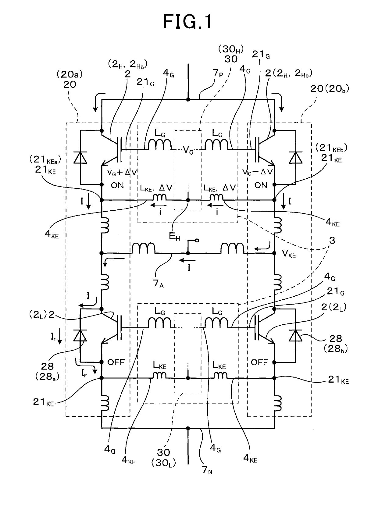
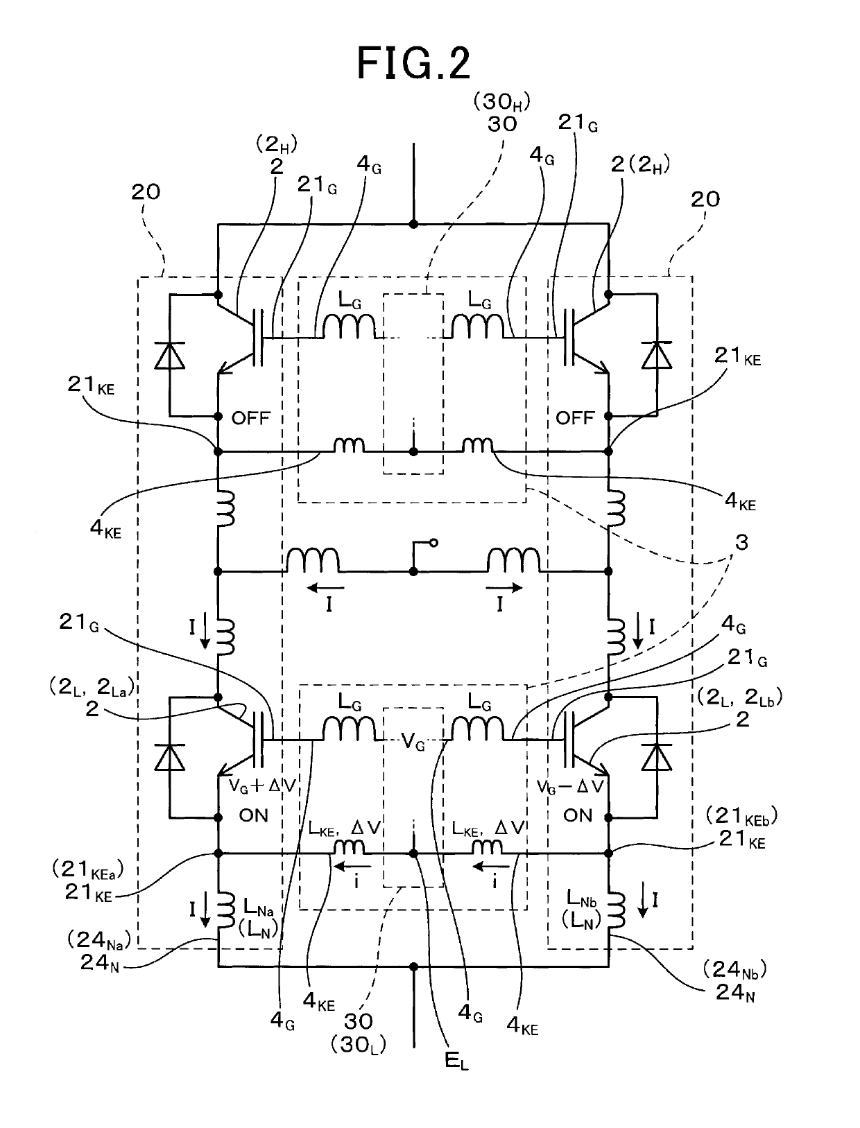
[0102]The present embodiment is an example in which a configuration of the semiconductor module 20 is changed. As illustrated in FIG. 12 and FIG. 13, in the present embodiment, the upper arm semiconductor elements 2H and the lower arm semiconductor elements 2L are incorporated into different semiconductor modules 20. In this case, as described above, while a difference is less likely to occur in potentials of the reference electrodes 21KE of a plurality of upper arm semiconductor elements 2H (see FIG. 12), there is a case where a difference occurs in potentials of the reference electrodes 21KE of the lower arm semiconductor elements 2L. That is, negative terminals 24N are connected to the reference electrodes 21KE of the lower arm semiconductor elements 2L, and it may occur that the inductances LNb of the negative terminals 24N vary. For example, it may occur that the inductance LNb of one lower arm semiconductor element 2Lb is larger than the inductance LNa of the other lower arm s...


PUM


Abstract

A plurality of semiconductor elements and a control circuit unit are provided. The plurality of semiconductor elements which are connected in parallel are configured to perform switching at the same time. The control circuit unit includes a drive circuit connected to the plurality of semiconductor elements which perform operation at the same time, control wirings and reference wirings. The control wirings connect control electrodes of the semiconductor elements to the drive circuit. The reference wirings connect reference electrodes of the semiconductor elements to the drive circuit. A parasitic inductance in the reference wiring is made smaller than a parasitic inductance in the control wiring.

Description

CROSS-REFERENCE TO RELATED APPLICATION[0001]The present application is based on and claims the benefit of priority from earlier Japanese Patent Application No. 2016-63541 filed on Mar. 28, 2016, and earlier Japanese Patent Application No. 2017-36745 filed on Feb. 28, 2017, the entire contents of which are incorporated herein by reference.TECHNICAL FIELD[0002]The present disclosure relates to a power conversion apparatus including a plurality of semiconductor elements and a control circuit unit which controls switching of the semiconductor elements.BACKGROUND ART[0003]As a power conversion apparatus which performs power conversion between DC power and AC power, a power conversion apparatus including semiconductor elements such as IGBTs and a control circuit unit electrically connected to the semiconductor elements, is known (see the following PTL 1). This power conversion apparatus is configured to convert DC power into AC power by causing the semiconductor elements to perform switch...

Claims


Application Information

Patent Timeline
Patent Type & Authority Applications(United States)
IPC IPC(8): H02M7/00H02M1/088H02M7/5387H02P27/06
CPCH02M7/003H02M1/088H02M7/5387H02P27/06H01L23/46H01L2224/0603H01L2924/00H01L2924/00014H01L23/49575H01L2224/45099H01L2924/13055H01L25/18H01L2224/48137
Inventor MIURA, TOMOYAYAMAHIRA, YUUFUKUSHIMA, KAZUMA
Owner DENSO CORP
Why Eureka
Try Eureka