Waveguide device module and microwave module

a technology of microwave modules and waveguides, applied in waveguides, waveguide fed arrays, instruments, etc., can solve the problems of difficulty in downsizing, need of fine processing, and the deterioration of the above-mentioned second structure, so as to reduce the loss of a waveguide

Inactive Publication Date: 2019-05-09
NIPPON DENSAN CORP +1
View PDF0 Cites 23 Cited by
  • Summary
  • Abstract
  • Description
  • Claims
  • Application Information

AI Technical Summary

Benefits of technology

[0016]According to an exemplary embodiment the present disclosure, it is possible to reduce losses in a waveguide extending from a microwave IC to a transmission / reception antenna.

Problems solved by technology

Against these demands, the aforementioned second structure has suffered from problems such as losses in the microstrip line, as well as difficulties of downsizing and needs of fine processing associated with the use of a hollow waveguide.

Method used


Image

  • Waveguide device module and microwave module
  • Waveguide device module and microwave module
  • Waveguide device module and microwave module

Examples


embodiment 1

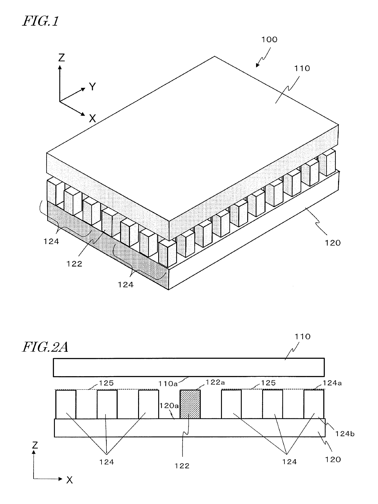
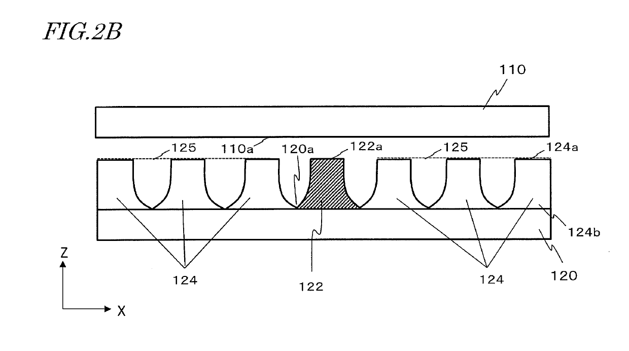
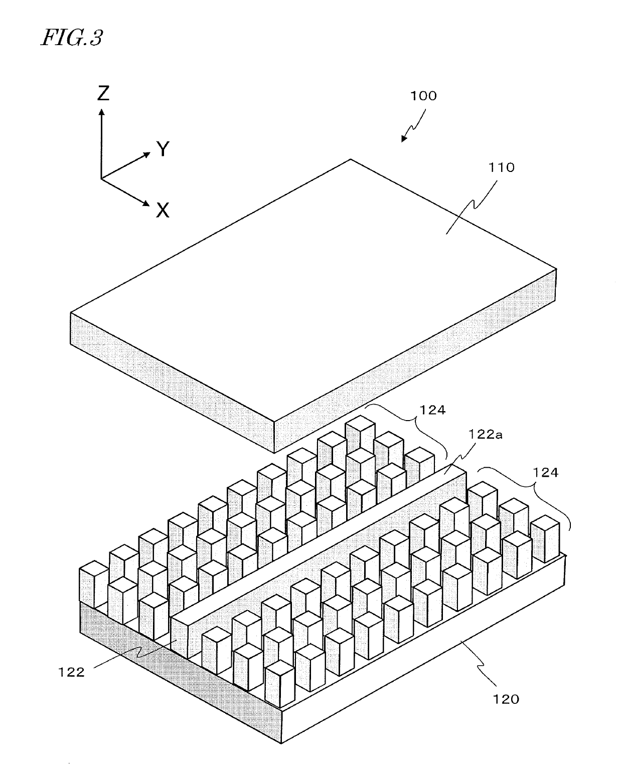
[0147]FIG. 9 shows an exemplary construction of a coupler 6 which mainly includes a ½ rectangular hollow-waveguide 30. In FIG. 9, (a) is an X-Y plan view (upper plan view) of the coupler 6; and (b) is a cross-sectional view taken along an XZ plane at line A-A′ in (a). Hereinafter, the +Z face of the coupler 6 will conveniently referred to as the “upper face”, and its −Z face as the “lower face”. In (b) of FIG. 9, an upper face 6a and a lower face 6b are shown.

[0148]First, the construction of the coupler 6 will be described. The coupler 6 can be produced by forming a thin electrically-conductive film on the surface of a base which is molded out of resin. The coupler 6 has one ½ rectangular hollow-waveguide 30 in the central portion of its upper face. A peripheral wall 32 is provided around the ½ rectangular hollow-waveguide 30. The peripheral wall 32 belongs in portions of the upper face of the coupler 6 other than the ½ rectangular hollow-waveguide 30. The end face in the +Z directi...

embodiment 2

[0190]FIG. 15 shows an exemplary construction of a microwave module 1001 including a coupler 6 according to the present embodiment. In FIG. 15, (a) shows an X-Y plan view of the coupler 6. In FIG. 15, (b) shows a cross-sectional view taken along an XZ plane at line u-u′ in (a). In FIG. 15, (c) shows a cross-sectional view taken along an XZ plane at line v-v′ in (a). Although not shown in FIG. 15, an artificial magnetic conductor as shown in FIG. 11B, for example, is provided in the +Y direction from the microwave module 1001. Details will be described with reference to FIGS. 18 and 19.

[0191]In the present embodiment, the coupler 6 of the microwave module 1001 includes two ½ rectangular hollow-waveguides 30 and 31 which are parallel to the X direction. Between the two ½ rectangular hollow-waveguides 30 and 31 is a protruding wall 38 having an upper face 6a of a flat strip shape. A peripheral wall 32 exists in the outer periphery of the coupler 6, the peripheral wall 32 having a flat ...

embodiment 3

[0215]FIG. 22 is an upper plan view a microwave module 1001 including a coupler 6 according to the present embodiment.

[0216]The coupler 6 according to the present embodiment includes a peripheral wall 32a, a ½ rectangular hollow-waveguide 230, a protruding wall 38a, a ½ rectangular hollow-waveguide 231, a protruding wall 38b, a ½ rectangular hollow-waveguide 232, and a peripheral wall 32b. Although the peripheral walls 32a and 32b are parted by a center line (broken line) with respect to the Y direction of the coupler 6, this is for convenience of illustration.

[0217]The ½ rectangular hollow-waveguide 230 is formed in a space which is interposed between the +Y side face of the protruding wall 38a, the −Y side face of the peripheral wall 32, and the bottom face. Moreover, the ½ rectangular hollow-waveguide 231 is formed in a space which is interposed between the −Y side face of the protruding wall 38a, the +Y side face of the protruding wall 38b, and the bottom face. The ½ rectangular...


PUM


Abstract

A waveguide device module includes a waveguide device including a conductor with an electrically conductive surface, a waveguide extending alongside the electrically conductive surface and including an electrically-conductive waveguide surface, and a first artificial magnetic conductor extending on both sides of the waveguide, a coupler including a first surface having a groove, a second surface opposite to the first surface, and a through hole extending from the first surface through to the second surface. The groove is connected at one end to the through hole and defined by first and second metal side surfaces opposing each other and a metal bottom surface connecting between the first and second metal side surfaces. A second artificial magnetic conductor at least opposes the groove. The first and second metal side surfaces, and the metal bottom surface define a ½ rectangular hollow-waveguide. The ½ rectangular hollow-waveguide and the waveguide device are connected via the through hole.

Description

CROSS REFERENCE TO RELATED APPLICATIONS[0001]This application claims the benefit of priority to Japanese Patent Application No. 2016-129340 filed on Jun. 29, 2016, Japanese Patent Application No. 2016-129341 filed on Jun. 29, 2016, Japanese Patent Application No. 2016-129342 filed on Jun. 29, 2016, Japanese Patent Application No. 2016-150513 filed on Jul. 29, 2016, Japanese Patent Application No. 2016-150514 filed on Jul. 29, 2016, Japanese Patent Application No. 2016-150515 filed on Jul. 29, 2016 and is a Continuation Application of PCT Application No. PCT / JP2017 / 023995 filed on Jun. 29, 2017. The entire contents of each application are hereby incorporated herein by reference.BACKGROUND OF THE INVENTION1. Field of the Invention[0002]The present disclosure relates to a waveguide device module, a microwave module, a radar device, and a radar system which guide electromagnetic waves by utilizing an artificial magnetic conductor.2. Description of the Related Art[0003]Microwaves (includ...

Claims


Application Information

Patent Timeline
Patent Type & Authority Applications(United States)
IPC IPC(8): H01Q1/32H01Q1/52H01Q21/00H01P3/123H01L23/66H01P5/107H01P3/08
CPCH01L2223/6677H01L2223/6633H01L2223/6616G01S13/931G01S2013/9392G01S13/867H01Q1/3233H01Q1/3283H01Q1/523H01Q21/005H01P3/123H01L23/66H01P5/107H01P3/081H01L2223/6683G01S7/03H01P5/12H01Q1/3291H01Q3/36H01Q21/064
Inventor KIRINO, HIDEKIKAMO, HIROYUKI
Owner NIPPON DENSAN CORP
Why Eureka
Try Eureka