Method of growing two-dimensional transition metal dichalcogenide thin film and method of manufacturing device including the same

a technology of transition metal dichalcogenide and thin film, which is applied in the direction of semiconductor devices, electrical equipment, transistors, etc., can solve the problems of difficult to grow two-dimensional materials of high quality to a uniform thickness on a wafer scale, process problems, etc., and achieve the effect of large area and higher quality

Active Publication Date: 2019-05-30
SAMSUNG ELECTRONICS CO LTD
View PDF2 Cites 5 Cited by
  • Summary
  • Abstract
  • Description
  • Claims
  • Application Information

AI Technical Summary

Benefits of technology

[0005]Provided are methods of growing a two-dimensional transition metal dichal...

Problems solved by technology

However, it is difficult to grow two-dimensional material having high quality to a uniform thickness on a wafer scale.
Although methods of using metal organic precursors have been in...

Method used


Image

  • Method of growing two-dimensional transition metal dichalcogenide thin film and method of manufacturing device including the same
  • Method of growing two-dimensional transition metal dichalcogenide thin film and method of manufacturing device including the same
  • Method of growing two-dimensional transition metal dichalcogenide thin film and method of manufacturing device including the same

Examples


Embodiment Construction

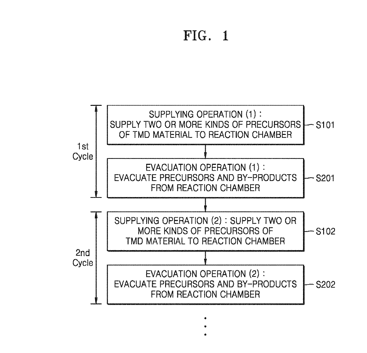
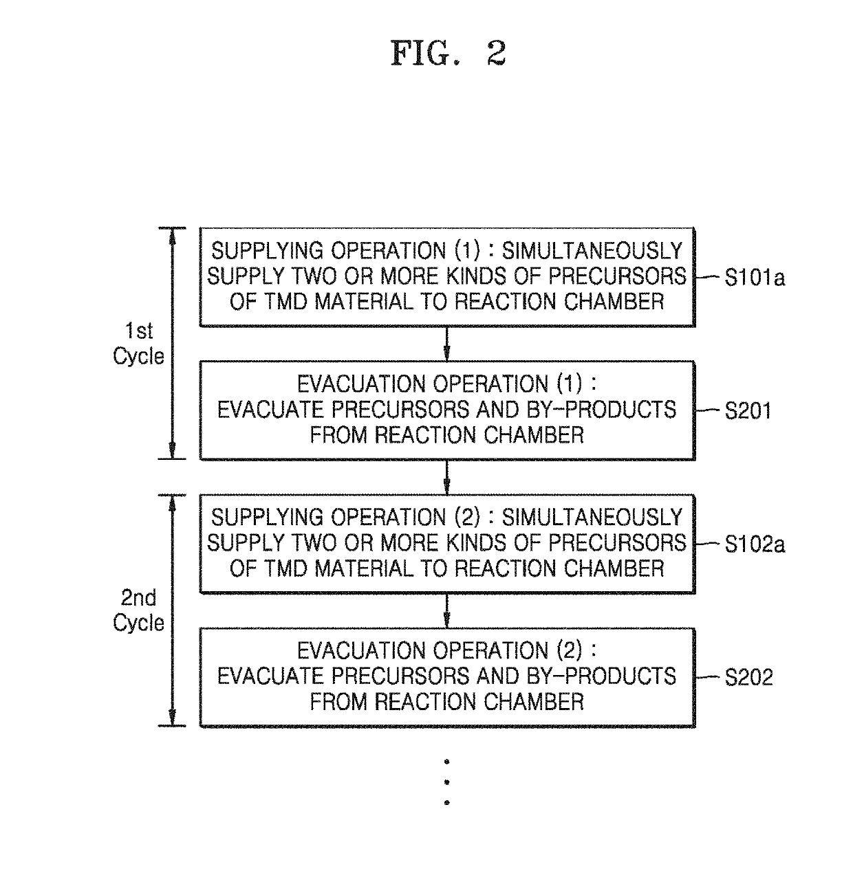
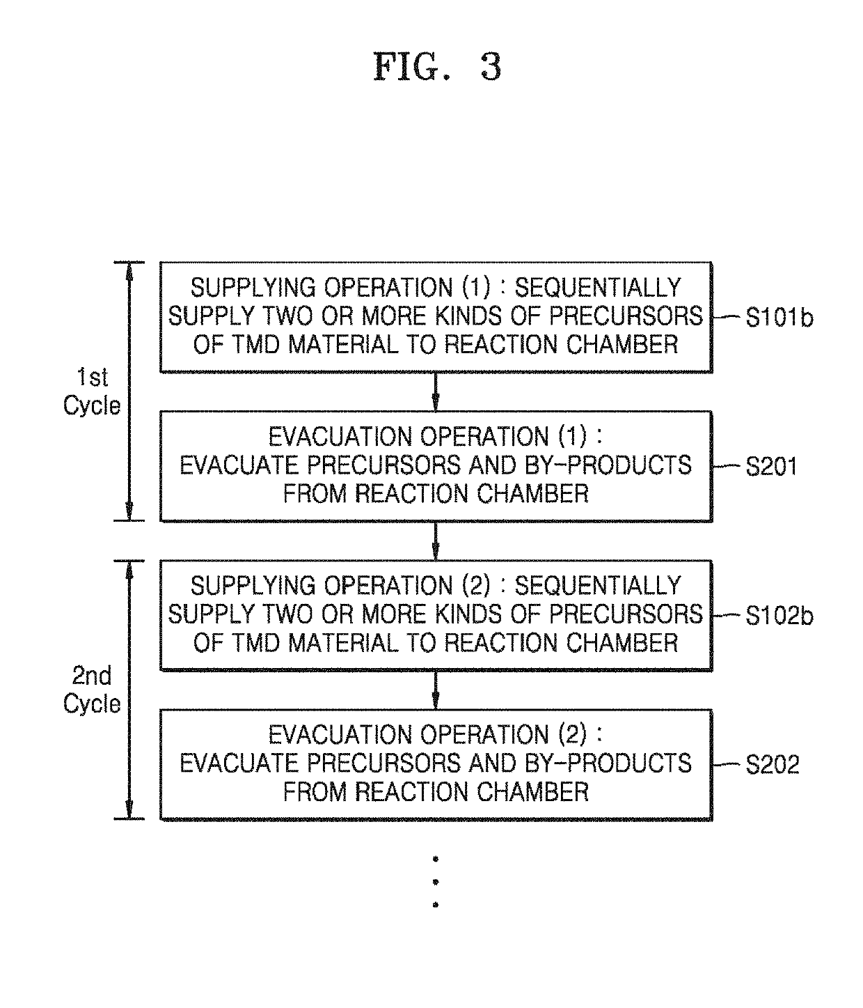
[0041]Various example embodiments will now be described more fully with reference to the accompanying drawings in which example embodiments are shown.

[0042]It will be understood that when an element is referred to as being “connected” or “coupled” to another element, it can be directly connected or coupled to the other element or intervening elements may be present. In contrast, when an element is referred to as being “directly connected” or “directly coupled” to another element, there are no intervening elements present. As used herein the term “and / or” includes any and all combinations of one or more of the associated listed items. Expressions such as “at least one of,” when preceding a list of elements, modify the entire list of elements and do not modify the individual elements of the list

[0043]It will be understood that, although the terms “first”, “second”, etc. may be used herein to describe various elements, components, regions, layers and / or sections, these elements, compon...


PUM


Abstract

A method of growing a two-dimensional transition metal dichalcogenide (TMD) thin film and a method of manufacturing a device including the two-dimensional TMD thin film are provided. The method of growing the two-dimensional TMD thin film may include a precursor supply operation and an evacuation operation, which are periodically and repeatedly performed in a reaction chamber provided with a substrate for thin film growth. The precursor supply operation may include supplying two or more kinds of precursors of a TMD material to the reaction chamber. The evacuation operation may include evacuating the two or more kinds of precursors and by-products generated therefrom from the reaction chamber.

Description

CROSS-REFERENCE TO RELATED APPLICATION[0001]This application claims the benefit of Korean Patent Application No. 10-2017-0161855, filed on Nov. 29, 2017, in the Korean Intellectual Property Office, the disclosure of which is incorporated herein in its entirety by reference.BACKGROUND1. Field[0002]The present disclosure relates to methods of growing a two-dimensional transition metal dichalcogenide (TMD) thin film and methods of manufacturing a device including the two-dimensional TMD thin film.2. Description of the Related Art[0003]A two-dimensional (2D) material is a single-layer or half-layer solid in which atoms form a crystal structure. An example of a typical two-dimensional material is graphene. Starting with research on graphene, research and development on various two-dimensional materials having semiconductor or insulator properties have been conducted. The two-dimensional materials are attracting attention as a next generation material that may overcome the limitation of e...

Claims


Application Information

Patent Timeline
IPC IPC(8): H01L21/02H01L29/66H01L29/786H01L29/24
CPCH01L21/02568H01L21/0262H01L29/66969H01L29/786H01L29/24H01L21/02376H01L21/02381H01L21/0242H01L21/02422H01L29/778H01L21/02485H01L21/02581H01L21/02205H01L21/02274H01L21/28568
Inventor KIM, HAERYONGSHIN, HYEONJINLEE, JAEHOJO, SANGHYUN
Owner SAMSUNG ELECTRONICS CO LTD
Why Eureka
Try Eureka