EVALUATION METHOD AND MANUFACTURING METHOD OF SiC EPITAXIAL WAFER

a manufacturing method and epitaxial wafer technology, applied in the direction of polycrystalline material growth, semiconductor/solid-state device testing/measurement, instruments, etc., can solve the problems of stacking faults, bpds in the sic substrate being converted into teds, and the device reliability is decreased

Active Publication Date: 2019-06-06
RESONAC CORP
View PDF2 Cites 3 Cited by
  • Summary
  • Abstract
  • Description
  • Claims
  • Application Information

AI Technical Summary

Benefits of technology

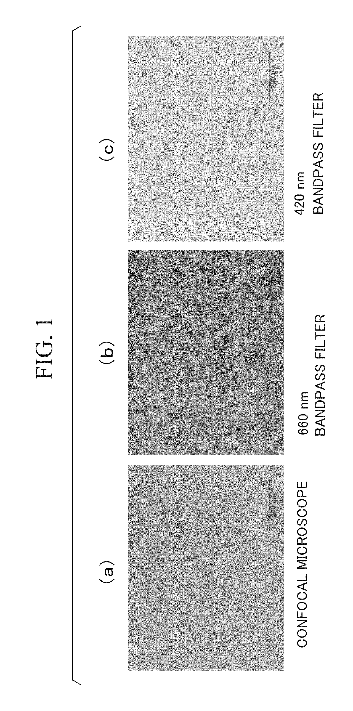
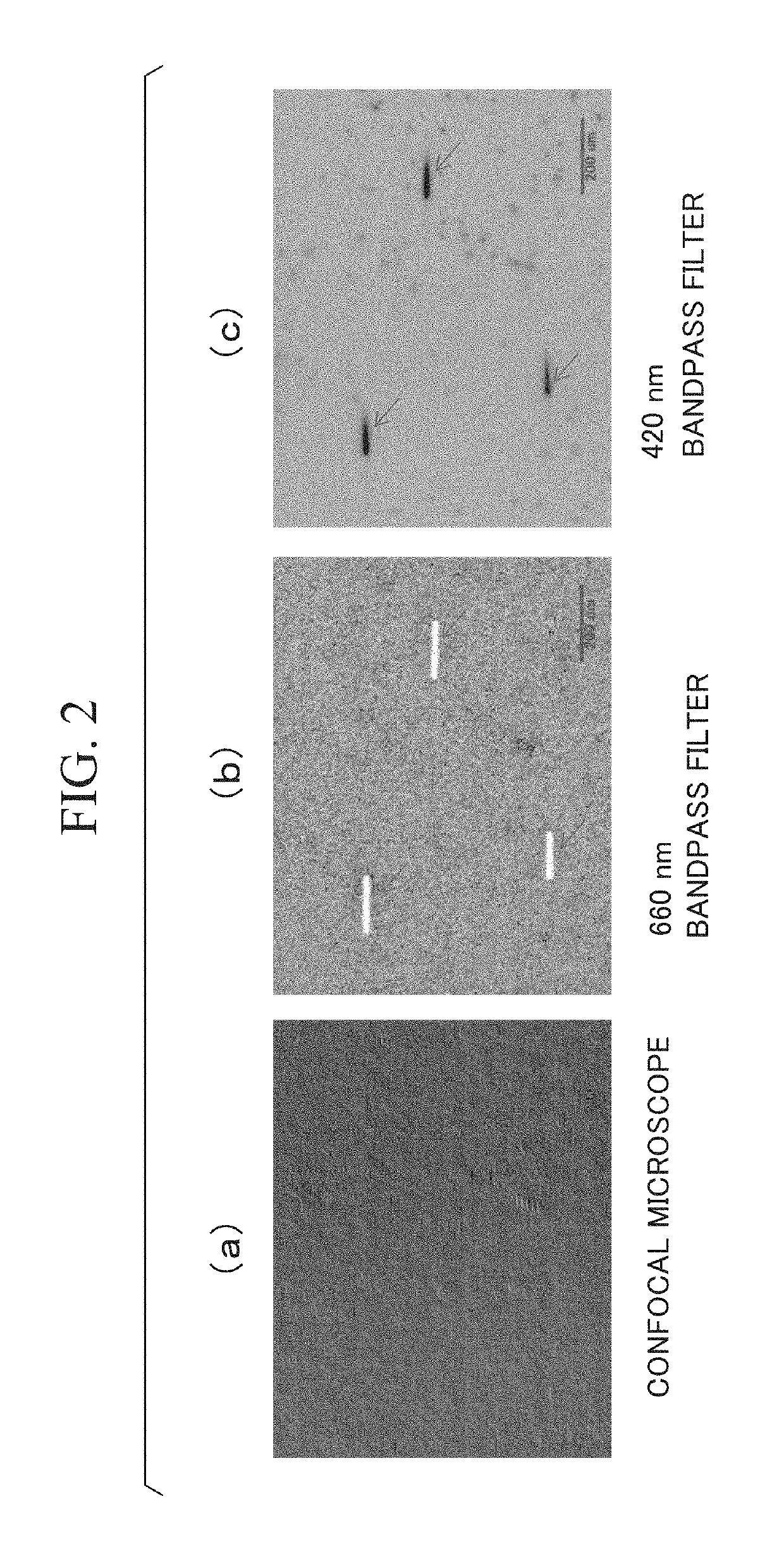
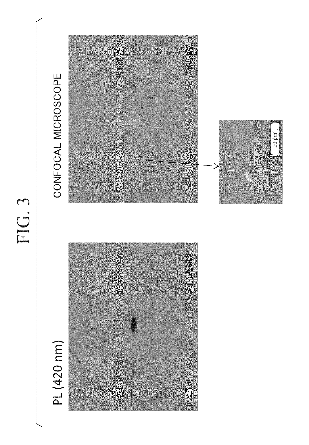
[0031]With the evaluation method of a SiC epitaxial wafer according to the aspect, it is possible to evaluate a basal plane dislocation (BPD) in the high-concentration epitaxial layer.

Problems solved by technology

In addition, when a high resistance portion is formed in the device, the reliability of the device is decreased.
On the other hand, it has been found that BPDs in the SiC substrate converted into TEDs form stacking faults in the epitaxial layer when a large current flows in a forward direction.

Method used


Image

  • EVALUATION METHOD AND MANUFACTURING METHOD OF SiC EPITAXIAL WAFER
  • EVALUATION METHOD AND MANUFACTURING METHOD OF SiC EPITAXIAL WAFER
  • EVALUATION METHOD AND MANUFACTURING METHOD OF SiC EPITAXIAL WAFER

Examples


Embodiment Construction

[0040]Hereinafter, an embodiment of the present invention will be described in detail with reference to the drawings as appropriate. In the drawings used in the following description, for ease of understanding of the features of the present invention, there are cases where characteristic portions are enlarged for convenience, and the dimension, the ratio and the like of each constituent element may be the same or may be different from reality. The materials, dimensions, and the like shown in the following description are merely examples, and the present invention is not limited thereto and can be embodied in appropriately modified manners in a range that does not change the gist thereof.

[0041]“Manufacturing Method of SiC Epitaxial Wafer”

[0042]A manufacturing method of a SiC epitaxial wafer according to the embodiment includes a step of stacking a high-concentration epitaxial layer having an impurity concentration of 1×1018 cm−3 or more on a SiC substrate, a step of evaluating the hi...


PUM


Abstract

An evaluation method of a SiC epitaxial wafer includes: a first observation step of preparing a SiC epitaxial wafer having a high-concentration epitaxial layer having an impurity concentration of 1×1018 cm−3 or more, irradiating a surface of the high-concentration epitaxial layer having an impurity concentration of 1×1018 cm−3 or more with excitation light, and observing a surface irradiated with the excitation light via a band-pass filter having a wavelength band of 430 nm or less.

Description

BACKGROUND OF THE INVENTIONField of the Invention[0001]The present invention relates to an evaluation method and a manufacturing method of a SiC epitaxial wafer.[0002]Priority is claimed on Japanese Patent Application No. 2017-234586, filed on Dec. 6, 2017, the content of which is incorporated herein by reference.Description of Related Art[0003]Silicon carbide (SiC) has a dielectric breakdown field larger by one order of magnitude, a band gap three times larger, and a thermal conductivity approximately three times higher than those of silicon (Si). Therefore, application of silicon carbide (SiC) to power devices, high-frequency devices, high-temperature operation devices, and the like is expected.[0004]In order to promote the practical application of SiC devices, establishment of high-quality SiC epitaxial wafers and high-quality epitaxial growth techniques is required.[0005]A SiC device is formed on a SiC epitaxial wafer including a SiC substrate and an epitaxial layer stacked on t...

Claims


Application Information

Patent Timeline
Patent Type & Authority Applications(United States)
IPC IPC(8): H01L21/66H01L21/02
CPCH01L22/12H01L21/02378H01L21/02529G01N21/9501G01N21/6489G01N2021/8461G01N2021/8477C30B29/00
Inventor NISHIHARA, YOSHITAKAKAMEI, KOJI
Owner RESONAC CORP
Why Eureka
Try Eureka