Phase-transition optical isomer compound, transparent electroluminescent display device and method of fabricating the transparent electroluminescent display device
- Summary
- Abstract
- Description
- Claims
- Application Information
AI Technical Summary
Benefits of technology
Problems solved by technology
Method used
Image
Examples
first embodiment
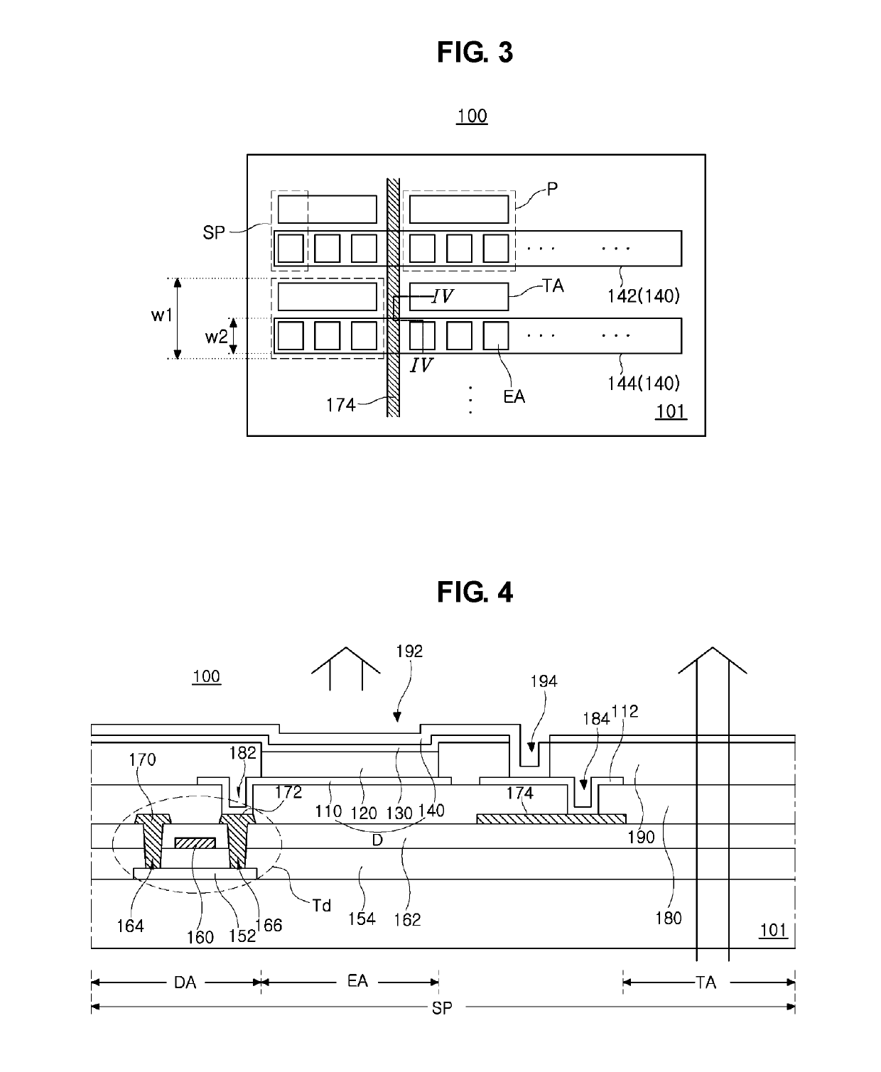
[0044]FIG. 3 is a schematic plane view of a transparent EL display device according to the present invention.
[0045]As shown in FIG. 3, the transparent EL display device 100 includes a plurality of sub-pixel regions (SP) defined on a substrate 110 and arranged along a first direction and a second direction. Each of the plurality of sub-pixel regions (SP) includes an emission area (EA) and a transparent area (TA). Each sub-pixel region (SP) further includes a driving area (not shown).
[0046]For example, some of the plurality of sub-pixel regions (SP) arrange along the first direction may constitute a pixel region (P). The pixel region (P) may include red, green and blue sub-pixel regions (SP).
[0047]In the emission area (EA) of the sub-pixel region (SP), an emitting diode (not shown) is disposed. For example, the emitting diode may include a first electrode, an emitting layer, an electron auxiliary layer and a second electrode 140.
[0048]As described below, the electron auxiliary layer i...
second embodiment
[0146]FIG. 9 is a schematic plane view of a transparent EL display device according to the present disclosure.
[0147]As shown in FIG. 9, the transparent EL display device 200 includes a plurality of sub-pixel regions (SP) defined on a substrate 210 and arranged along a first direction and a second direction. Each of the plurality of sub-pixel regions (SP) includes an emission area (EA) and a transparent area (TA). Each sub-pixel region (SP) further includes a driving area (not shown).
[0148]For example, some of the plurality of sub-pixel regions (SP) that arrange along the first direction may constitute a pixel region (P). The pixel region (P) may include red, green and blue sub-pixel regions (SP).
[0149]In the emission area (EA) of the sub-pixel region (SP), an emitting diode (not shown) is disposed. For example, the emitting diode may include a first electrode, an emitting layer, an electron auxiliary layer and a second electrode 240.
[0150]As described below, the electron auxiliary l...
PUM
| Property | Measurement | Unit |
|---|---|---|
| Glass transition temperature | aaaaa | aaaaa |
| Electrical conductor | aaaaa | aaaaa |
| Area | aaaaa | aaaaa |
Abstract
Description
Claims
Application Information
 - R&D Engineer
- R&D Manager
- IP Professional
- Industry Leading Data Capabilities
- Powerful AI technology
- Patent DNA Extraction
Browse by: Latest US Patents, China's latest patents, Technical Efficacy Thesaurus, Application Domain, Technology Topic, Popular Technical Reports.
© 2024 PatSnap. All rights reserved.Legal|Privacy policy|Modern Slavery Act Transparency Statement|Sitemap|About US| Contact US: help@patsnap.com


