Electron source and production method therefor

a technology of electron emission material and production method, which is applied in the direction of electric discharge tube, discharge tube/lamp details, discharge tube coating, etc., can solve the problem that the consumption of electron emission material cannot be sufficiently suppressed based on the techniques, and achieve the effect of suppressing the consumption of electron emission material

Active Publication Date: 2019-07-18
DENKA CO LTD
View PDF1 Cites 4 Cited by
  • Summary
  • Abstract
  • Description
  • Claims
  • Application Information

AI Technical Summary

Benefits of technology

[0013]According to the present invention, the consumption of the electron emission material can be suppressed.

Problems solved by technology

When the present inventors investigated the techniques described in the above documents, it was found that, in some conditions, consumption of the electron emission material could not be sufficiently suppressed based on the techniques described in the above documents.

Method used


Image

  • Electron source and production method therefor
  • Electron source and production method therefor
  • Electron source and production method therefor

Examples


example 1

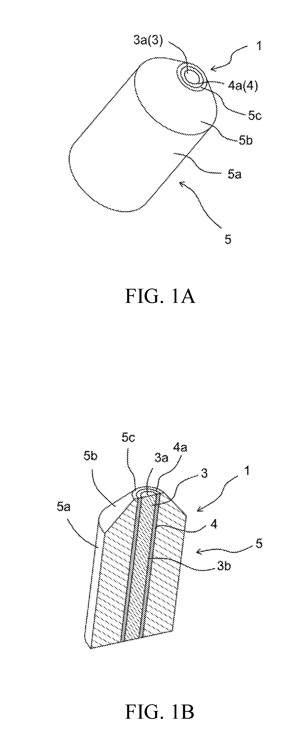
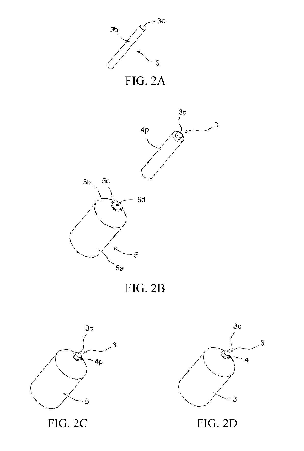
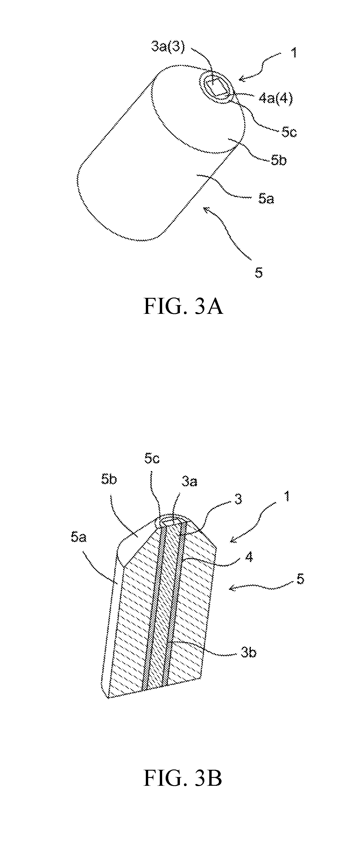
[0053]As an electron emission material 3, a cylindrical rod having a shape of a diameter of 0.1 mm×a height of 1 mm with a longitudinal axis of direction was produced from a single crystal of lanthanum boride by electric discharge machining. It was difficult to limit crystal orientation of side surface thereof, but it was about 45 degrees off (100).

[0054]Next, high-purity graphite having a quadrangular prism shape of 0.7 mm×0.7 mm×1.2 mm was prepared and then an end part thereof was sharpened by machining to prepare a support member 5. An opening 5d having a diameter of 0.15 mm×a depth of 0.8 mm was formed in the longitudinal direction of the support member by machining

[0055]Paste 4p obtained by dissolving tantalum powder as an electron emission-suppressing material 4 with water was applied to a side surface 3b of the electron emission material 3. Then, the electron emission material 3 having the applied paste 4p was inserted into the opening 5d of the support member 5.

[0056]Heater...

examples 2 to 3

[0059]Each of electron source 1 was produced in the same manner as in Example 1 except that powder obtained by mixing tantalum powder and boron carbide (product name: Denka Boron Carbide #1000) at a volume ratio shown in Table 2 was used as the electron emission-suppressing material 4 instead of the tantalum powder and that the temperature at which the paste 4p was solidified was changed to 1550° C.

example 4

[0060]An electron source 1 was obtained in the same manner as in Example 1 except that cerium boride was used as the electron emission material 3 instead of lanthanum boride.


PUM


Abstract

An electron source capable of suppressing consumption of an electron emission material is provide. The present invention provides an electron source including: an electron emission material; and, an electron emission-suppressing material covering a side surface of the electron emission material, wherein a work function of the electron emission-suppressing material is higher than that of the electron emission material, and a thermal emissivity of the electron emission-suppressing material is lower than that of the electron emission material.

Description

TECHNICAL FIELD[0001]The present invention relates to an electron source used in an electron microscope, an electron beam lithography apparatus, a semiconductor photomask plotting apparatus and the like using an electron beam, and a production method thereof.BACKGROUND ART[0002]Patent documents 1 to 6 and non-patent document 1 disclose a technique for limiting a electron-emitting region by covering a periphery of an electron emission material with graphite material in an electron source, thereby enabling enhancement of luminance and suppression of surplus current.PRIOR ART DOCUMENTSNon-Patent Document[0003][Non-Patent Document 1] Electron Optical Systems (pp. 163-170) SEM Inc., AMF O'Hare (Chicago), IL 60666-0507, U.S. Pat. S. A.Patent Documents[Patent Document 1] JP2005-228741A[Patent Document 2] JP2005-190758A[Patent Document 3] JP2000-173900A[Patent Document 4] JP2009-152645A[Patent Document 5] JP2012-069364A[Patent Document 6] JP2014-075336ASUMMARY OF THE INVENTIONProblems to be...

Claims


Application Information

Patent Timeline
Patent Type & Authority Applications(United States)
IPC IPC(8): H01J37/06H01J1/148H01J9/04
CPCH01J37/06H01J1/148H01J9/04H01J2209/012H01J2201/30426H01J2237/06341H01J9/025
Inventor MORISHITA, TOSHIYUKICHATANI, HIROMITSUHIROKAWA, SHIMPEIIBAYASHI, TOSHIYUKISUGIMOTO, ISAO
Owner DENKA CO LTD
Why Eureka
Try Eureka