Laser color marking method for a semiconductor package
a color marking and semiconductor technology, applied in semiconductor devices, semiconductor/solid-state device details, electrical devices, etc., can solve the problems of high ink printing cost, abnormal condition of semiconductor packages, damage to the internal structure of semiconductor elements b>50/b>, etc., and achieve the effect of easy formation of visible color marks
- Summary
- Abstract
- Description
- Claims
- Application Information
AI Technical Summary
Benefits of technology
Problems solved by technology
Method used
Image

Examples
first embodiment
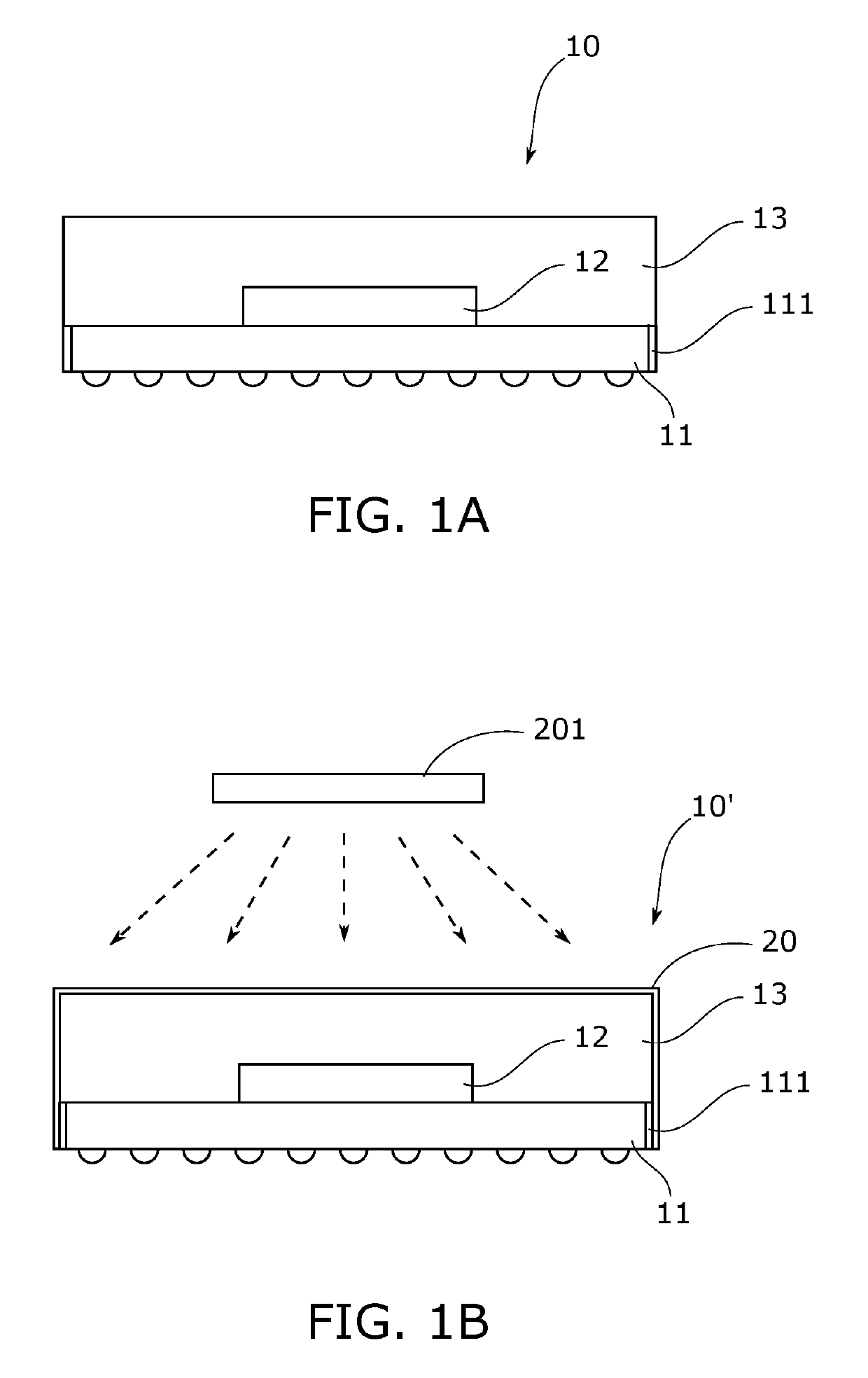
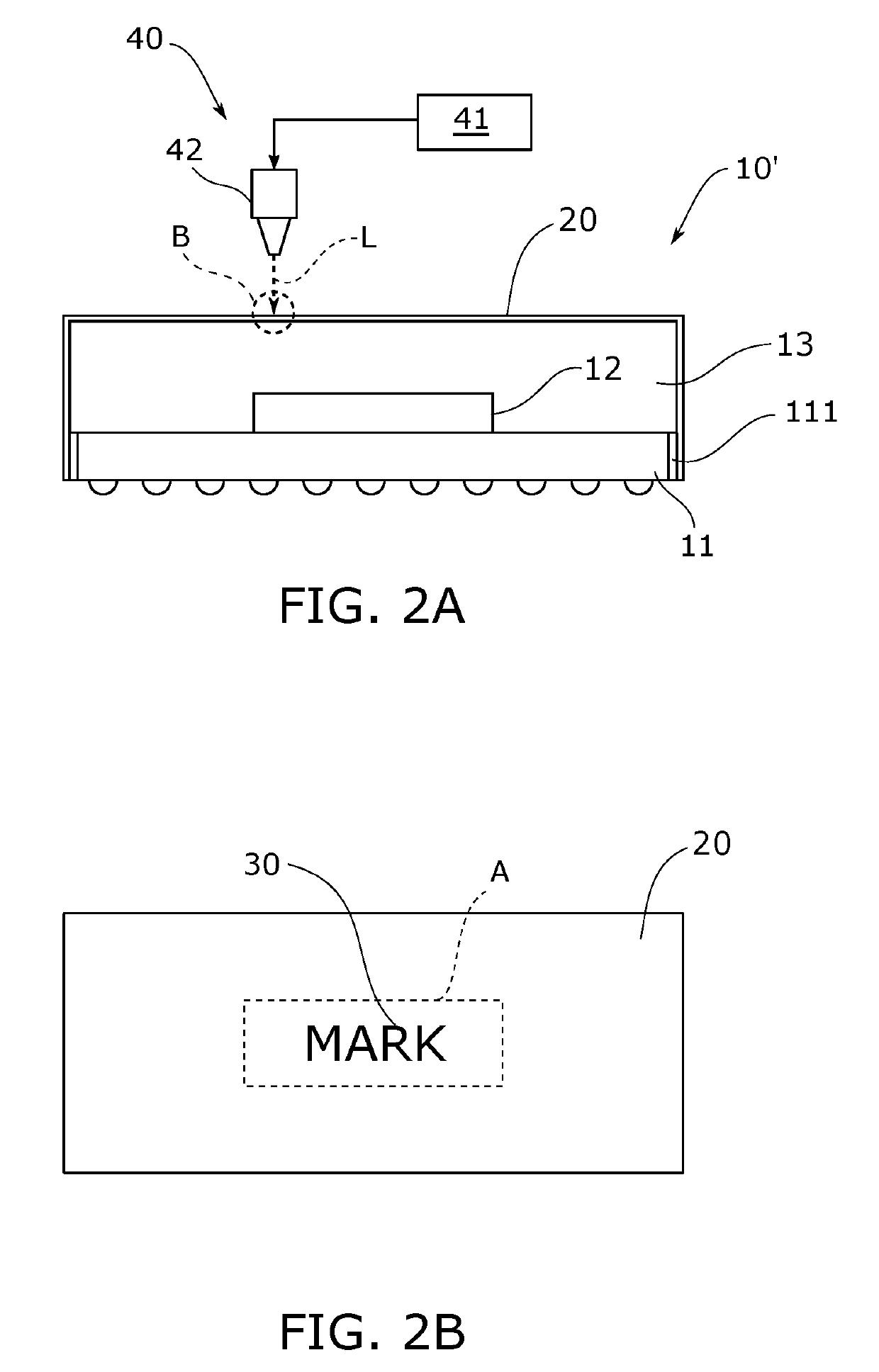
[0035]With reference to FIGS. 1A and 4A, the laser color mark method is shown and has steps of: (a) providing a semiconductor element 10 (S11); (b) forming a metal layer 20 on the semiconductor element 10 (S12), as shown in FIG. 1B; (c) obtaining a marking pattern (S13); and (d) applying a laser light L on the metal layer 20 to form a mark 30 according to the marking pattern (S14), as shown in FIGS. 2A and 2B.
[0036]With reference to FIG. 1A, in the step (a) S11, the semiconductor element 10 has a substrate 11 with at least one chip 12 mounted onto the substrate 10 and an encapsulation 13 encapsulating the chip 12 and on top of the substrate 11. The substrate 11 has a ground pad 111 electronically connected to the ground of an IC system power.
[0037]With further reference to FIG. 1B, an alloy material 201 is formed on the semiconductor element 10. The alloy material 201 may be formed on the semiconductor element 10 through sputtering in a sputtering chamber (not shown). In the sputter...
second embodiment
[0047]With reference to FIGS. 1 and 4B, the laser color marking method of the present invention is shown and has steps of: (a) providing a semiconductor element 10 that has an outer alloy metal layer 20 and a surface of the outer alloy metal layer 20 has a marking region A (S21); (b) obtaining a marking pattern (S22); and (c) applying a laser light L on the marking region A to form mark 30 (S23), as shown in FIGS. 2A and 2B.
[0048]The outer alloy metal layer 20 may be made of an alloy material, such as SUS 304. When the laser light supplies to the metal layer 20 that is made of SUS 304, the optical oxide layer thereof converts a corresponding color light, as mentioned above.
[0049]Based on the foregoing description, in the laser color marking method, the metal layer is directly formed on the semiconductor element by a sputtering process. The laser light is directly provided on a surface of the metal layer to form an optical oxide film to convert the ambient light to the corresponding ...
PUM
 Abstract
Description
Claims
Application Information
 - Generate Ideas
- Intellectual Property
- Life Sciences
- Materials
- Tech Scout
- Unparalleled Data Quality
- Higher Quality Content
- 60% Fewer Hallucinations
Browse by: Latest US Patents, China's latest patents, Technical Efficacy Thesaurus, Application Domain, Technology Topic, Popular Technical Reports.
© 2025 PatSnap. All rights reserved.Legal|Privacy policy|Modern Slavery Act Transparency Statement|Sitemap|About US| Contact US: help@patsnap.com