Carbon film gapfill for patterning application

a technology of carbon film and patterning, applied in the direction of semiconductor/solid-state device manufacturing, basic electric elements, electric apparatus, etc., can solve the problem of inability to meet the trend of smaller feature sizes of devices

Inactive Publication Date: 2019-08-01
APPLIED MATERIALS INC
View PDF0 Cites 160 Cited by
  • Summary
  • Abstract
  • Description
  • Claims
  • Application Information

AI Technical Summary

Problems solved by technology

However, there are demands and device trends for s...

Method used


Image

  • Carbon film gapfill for patterning application
  • Carbon film gapfill for patterning application
  • Carbon film gapfill for patterning application

Examples


Embodiment Construction

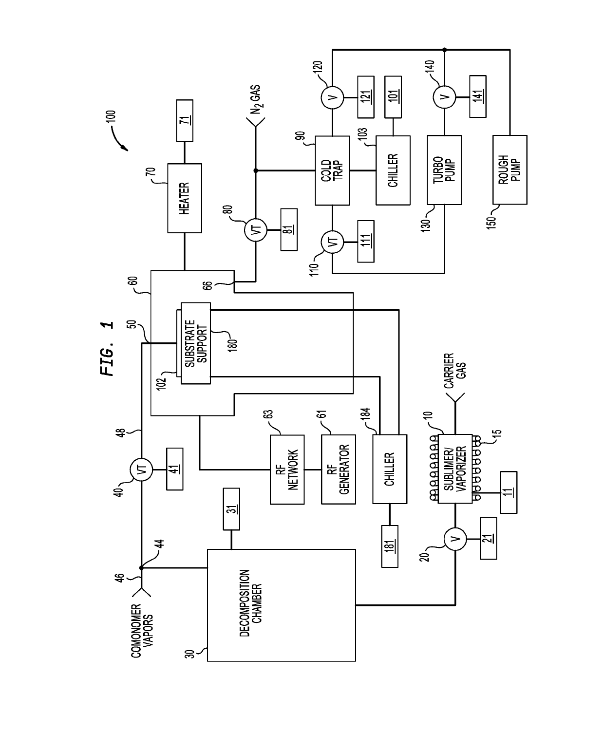
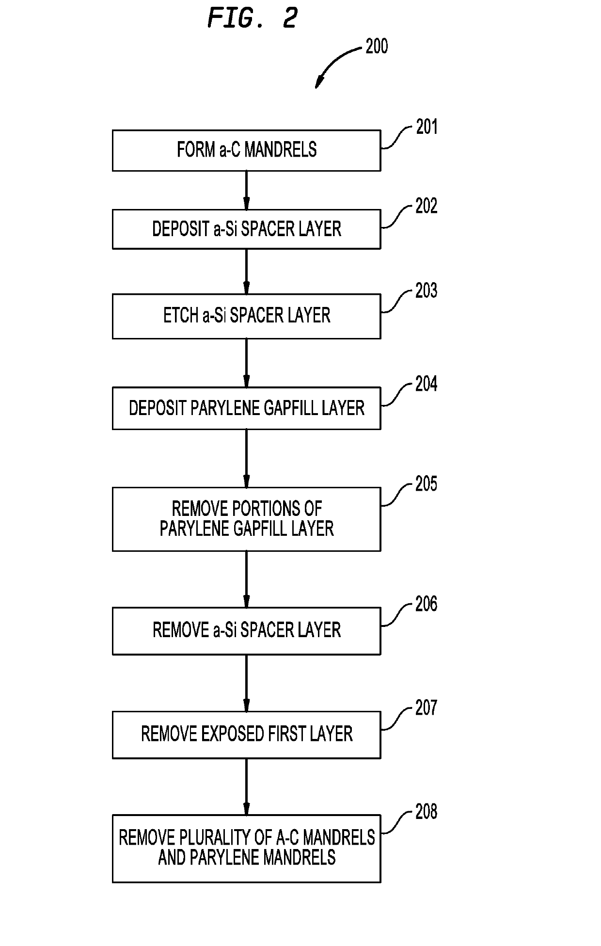
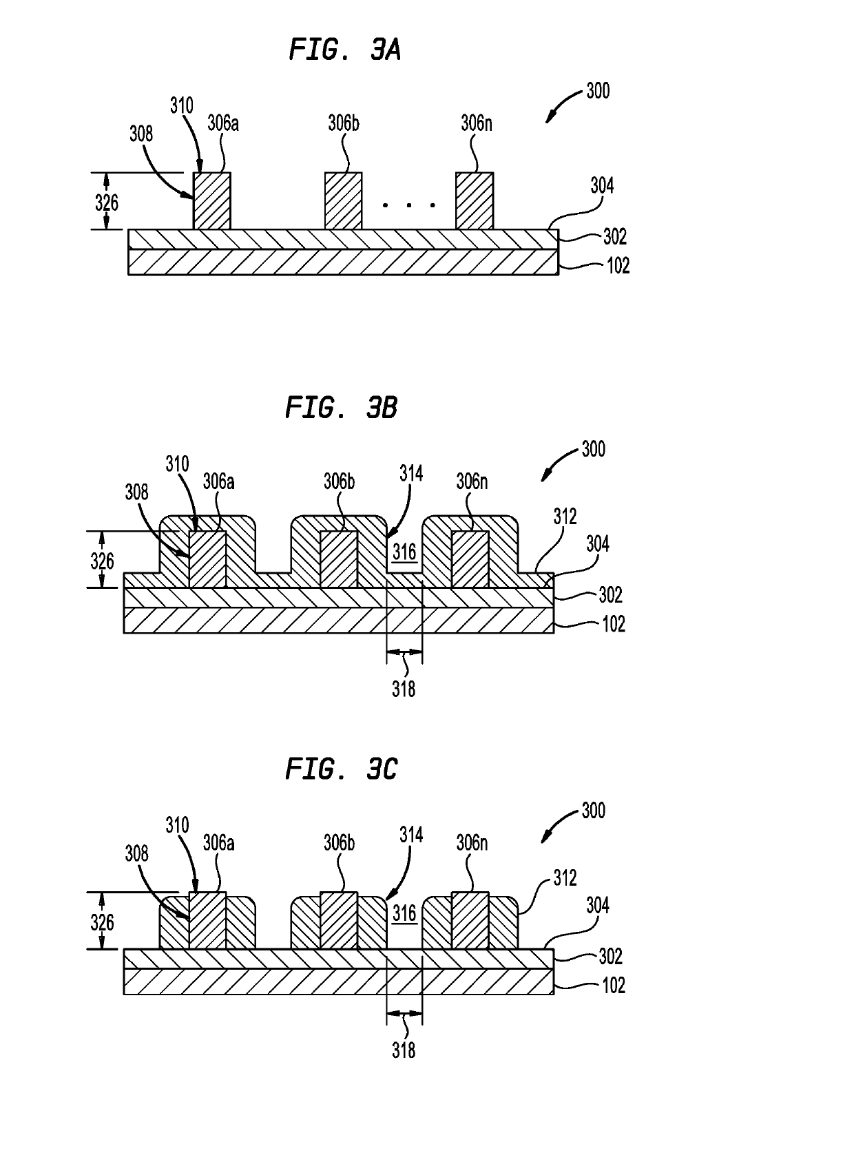
[0018]Embodiments described herein relate to methods for forming patterns of semiconductor devices utilizing parylene gapfill layers deposited using a thermal chemical vapor deposition (CVD) process. In one embodiment the patterns of semiconductor devices are formed by forming amorphous carbon (a-C) mandrels on first layers, depositing amorphous silicon (a-Si) layers over the a-C mandrels and the first layers, etching the a-Si spacer layers to expose top surfaces of the a-C mandrels and to expose the first layers, depositing parylene gapfill layers using the CVD process, removing portions of the parylene gapfill layers until the top surfaces are exposed; and removing the a-Si spacer layers to expose the first layers and form patterns of semiconductor devices having a-C mandrels and parylene mandrels.

[0019]As used herein, the term “parylene” is the generic name for thermoplastic polymers based on p-xylylene (CH2C6H4CH2) or derivatives of the parylene monomers, polymers, or copolymers...


PUM


Abstract

Embodiments described herein relate to methods for forming patterns of semiconductor devices utilizing parylene gapfill layers deposited using a thermal chemical vapor deposition (CVD) process. In one embodiment the patterns of semiconductor devices are formed by forming amorphous carbon (a-C) mandrels on first layers, depositing amorphous silicon (a-Si) layers over the a-C mandrels and the first layers, etching the a-Si spacer layers to expose top surfaces of the a-C mandrels and to expose the first layers, depositing parylene gapfill layers using the CVD process, removing portions of the parylene gapfill layers until the top surfaces are exposed; and removing the a-Si spacer layers to expose the first layers and form patterns of semiconductor devices having a-C mandrels and parylene mandrels.

Description

BACKGROUNDField[0001]Embodiments of the present disclosure generally relate to methods for forming patterns of semiconductor devices. More particularly, embodiments of the present disclosure relate to pattern forming methods utilizing a parylene gapfill layer deposited using a thermal CVD process.Description of the Related Art[0002]Semiconductor device processing is used to create integrated circuits that are present in electrical devices.[0003]Conventionally, in the fabrication of integrated circuits, photo lithography scanners using 193 nanometer (nm) wavelength lasers and numerical apertures of 1.35 have reached fundamental printing limits of 40 nm to 45 nm. However, there are demands and device trends for smaller feature sizes not obtainable by photo lithography. Multi-color patterning processes are used to form lines, vias, trenches, contacts, devices, gates and other features on substrates Multi-color patterning processes form smaller features not obtainable by photo lithograp...

Claims


Application Information

Patent Timeline
IPC IPC(8): H01L21/027H01L21/033H01L21/311
CPCH01L21/0273H01L21/0332H01L21/31138H01L21/0335H01L21/31116H01L21/02118H01L21/02271H01L21/0337
Inventor WANG, FEIWANG, MIAOJUNJIANG, SHISHIMANNA, PRAMITMALLICK, ABHIJIT BASUVISSER, ROBERT JAN
Owner APPLIED MATERIALS INC
Why Eureka
Try Eureka