Semiconductor device and method for fabricating the same

a semiconductor and semiconductor technology, applied in the direction of transistors, optics, instruments, etc., can solve the problems of poor smoothness and difficulty in electric current flow, and achieve the effects of reducing mobility, reducing and improving carrier mobility in the channel layer

Active Publication Date: 2005-01-06
PANASONIC CORP
View PDF9 Cites 50 Cited by
  • Summary
  • Abstract
  • Description
  • Claims
  • Application Information

AI Technical Summary

Benefits of technology

However, according to Document 1, with the use of such an off substrate, if a channel layer of a MISFET is provided to be in parallel with the principal surface of the substrate, the carrier mobility in the channel layer is decreased, and if the channel layer is provided to be perpendicular to the principal surface in an off direction, the carrier mobility in the channel layer is improved. This is because a step exists at a surface of the off substrate, and it becomes difficult for electric current to flow if a channel is set in a direction traversing this step. In other words, the mobility is decreased due to the irregularities of the surface.

Problems solved by technology

This is because a step exists at a surface of the off substrate, and it becomes difficult for electric current to flow if a channel is set in a direction traversing this step.
Therefore, the surface roughness of the channel layer 135 is also aggravated, and thus the smoothness thereof is also poor.

Method used


Image

  • Semiconductor device and method for fabricating the same
  • Semiconductor device and method for fabricating the same
  • Semiconductor device and method for fabricating the same

Examples


first embodiment

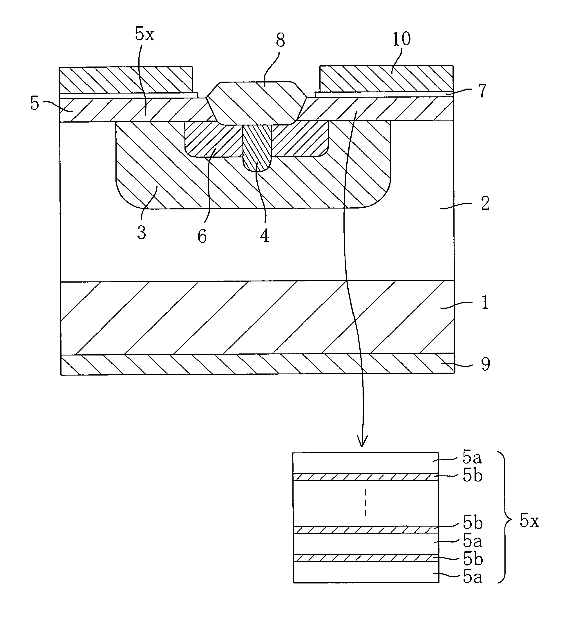
In the present embodiment, an accumulation-mode double-implantation MISFET that uses a bulk SiC substrate will be described as a first embodiment of the present invention. FIG. 1 is a cross-sectional view illustrating the structure of the double-implantation MISFET according to the first embodiment of the present invention. Although FIG. 1 shows only a partial cross-sectional structure of the MISFET, the planar structure thereof is similar to one disclosed in FIG. 2 or 10 of International Application PCT / JP01 / 07810, for example.

As shown in FIG. 1, the double-implantation MISFET includes: a low resistance SiC substrate 1 containing an n-type dopant at a concentration of 1×1018 cm−3 or more; a high resistance SiC layer 2 provided on a principal surface of the SiC substrate 1 and containing an n-type dopant at a concentration of about 1×1015 cm−3 to about 1×1016 cm−3; a p-well region 3 formed by doping a part of a surface region of the high resistance SiC layer 2 with a p-type dopan...

second embodiment

A semiconductor device according to a second embodiment of the present invention has a structure apparently similar to that of the double-implantation MISFET in the first embodiment shown in FIG. 1, and therefore, the structure of the MISFET according to the second embodiment is not shown. The MISFET of the present embodiment is greatly different from that of the first embodiment in that the surfaces of the high resistance SiC layer 2, the well region 3 and the source region 6 are not smoothed, and the surface smoothness is maintained by activation annealing performed with the high resistance SiC layer 2, the well region 3 and the source region 6 covered with a carbon film. Furthermore, the epitaxially grown layer 5 including the channel layer 5x is epitaxially grown on the high resistance SiC layer 2, the well region 3 and the source region 6. The channel layer 5x (the epitaxially grown layer 5) according to the present embodiment has an internal structure similar to that of the c...

third embodiment

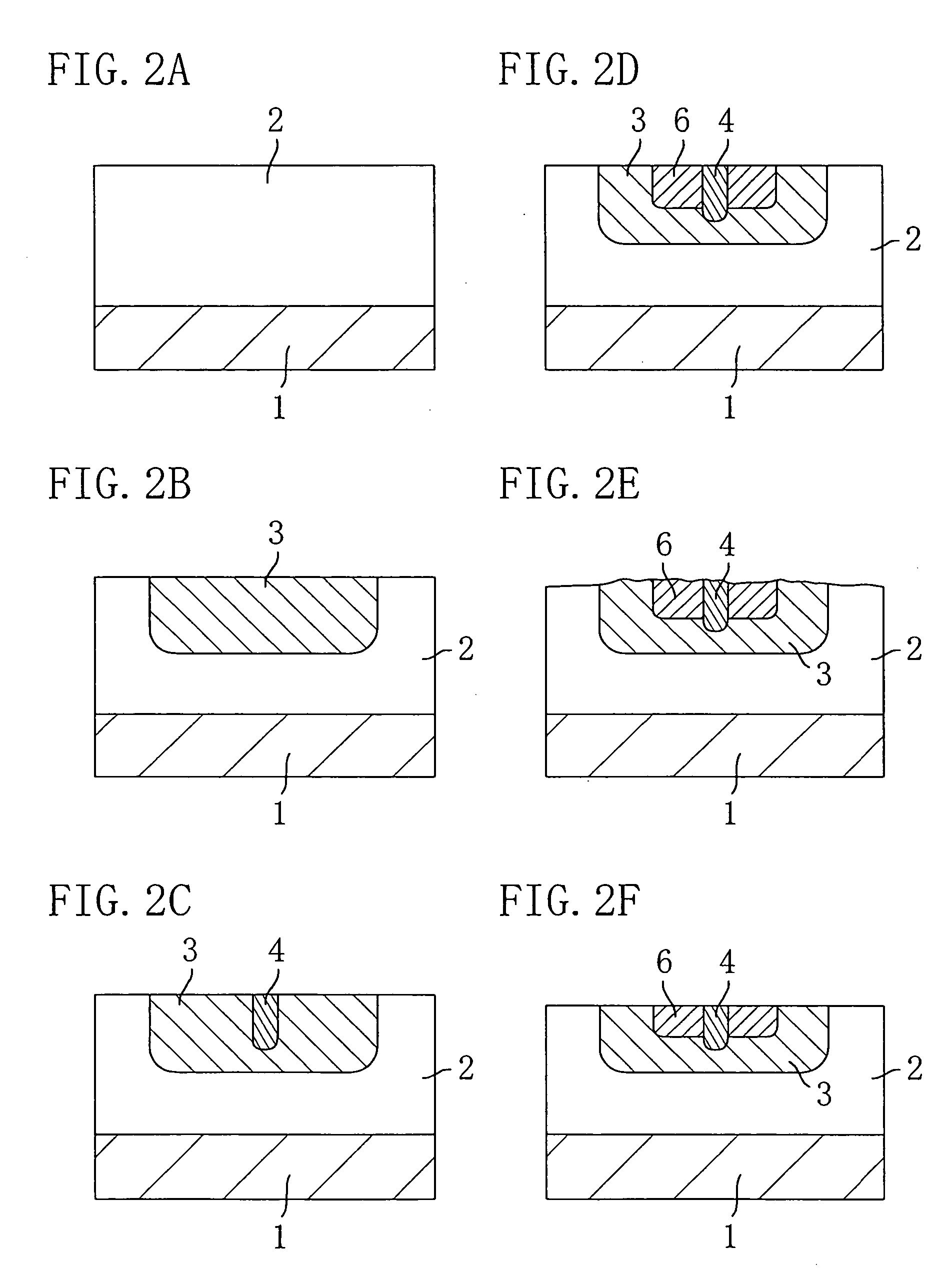
FIGS. 6A through 6F are cross-sectional views illustrating the process for fabricating a double-implantation MISFET according to a third embodiment of the present invention.

First, in the step shown in FIG. 6A, the step similar to that shown in FIG. 2A according to the first embodiment is carried out, thus epitaxially growing a high resistance SiC layer 2 on a principal surface of a SiC substrate 1 that is an off-substrate having an off angle of 8° from the (0001) plane of 4H—SiC.

Next, in the step shown in FIG. 6B, the step similar to that shown in FIG. 2C according to the first embodiment is carried out. Thus, a p+ contact region 4 is formed by implanting high-concentration p-type dopant ions into a part of a surface region of the high resistance SiC layer 2 in order to allow a p-well region and a source electrode, which will be subsequently formed, to be in electrical contact with each other. The p+ contact region 4 has a dopant concentration of about 5×1019 cm−3 or more.

Ther...


PUM

PropertyMeasurementUnit
surface roughnessaaaaaaaaaa

Abstract

Ion implantation is carried out to form a p-well region and a source region in parts of a high resistance SiC layer on a SiC substrate, and a carbon film is deposited over the substrate. With the carbon film deposited over the substrate, annealing for activating the implanted dopant ions is performed, and then the carbon film is removed. Thus, a smooth surface having hardly any surface roughness caused by the annealing is obtained. Furthermore, if a channel layer is epitaxially grown, the surface roughness of the channel layer is smaller than that of the underlying layer. Since the channel layer having a smooth surface is provided, it is possible to obtain a MISFET with a high current drive capability.

Description

BACKGROUND OF THE INVENTION The present invention relates to a power device that utilizes a silicon carbide substrate (SiC substrate) used to handle high voltages and high currents. Conventionally, a power device has been desired to be low-loss since it is a semiconductor device that handles high voltages and high currents. In the prior art, a power device that uses a silicon (Si) substrate has been the prevailing device. However, in recent years, a power device that uses a SiC (silicon carbide) substrate made of a semiconductor material containing Si and C in the ratio 1:1 is getting attention and being developed. Since the dielectric breakdown field of SiC is ten times greater than that of silicon, SiC makes it possible to maintain high reverse blocking voltage even if a depletion layer at a pn junction or a Schottky junction is thinned. Therefore, if a SiC substrate is used, the thickness of the resulting device can be reduced, and dopant concentration can be increased. Accordi...

Claims


Application Information

Patent Timeline
Patent Type & Authority Applications(United States)
IPC IPC(8): H01L21/04H01L29/10H01L29/15H01L29/24H01L29/36H01L29/78H01L29/812
CPCH01L21/046H01L21/0475H01L21/0485H01L21/30625H01L29/1029H01L29/105H01L29/812H01L29/365H01L29/41766H01L29/66068H01L29/7828H01L29/7838H01L29/1608
Inventor KUSUMOTO, OSAMUKITABATAKE, MAKOTOUCHIDA, MASAOTAKAHASHI, KUNIMASAYAMASHITA, KENYAHAGIO, MASAHIROSAWADA, KAZUYUKI
Owner PANASONIC CORP
Why Eureka
Try Eureka