
A semiconductor logic element and logic circuitries

Active Publication Date: 2019-08-08
HYPERION SEMICON OY
View PDF1 Cites 0 Cited by
  • Summary
  • Abstract
  • Description
  • Claims
  • Application Information

AI Technical Summary

Benefits of technology

The invention introduces new semiconductor logic elements with lower power consumption than traditional semiconductor logic elements. These elements can replace traditional semiconductor logic elements in complementary logic. The invention provides a semiconductor logic element comprising a field effect transistor of the first conductivity type and a field effect transistor of the second conductivity type. The semiconductor logic element has an internal node that can adjust to different potentials to establish a conductive channel. The semiconductor logic element can be a depletion mode field effect transistor or an enhancement mode field effect transistor. The invention also provides a method for designing these semiconductor logic elements.

Problems solved by technology

In addition, it is only possible in complementary binary logic to establish a network of logic elements having the outputs of logic elements connected to the inputs of other logic elements and wherein the inputs / outputs of logic elements are biased only at a two different potentials that are the same throughout the network.
It is possible to have individual auxiliary gate nodes for both type CISFETs by incorporating underneath the CISFETs an insulator layer and by incorporating deep enough trenches that reach to this insulator layer but this would increase the cost.
The back-gate doping can be connected also to the source of the corresponding CISFET but in this case the ability to adjust the threshold voltage is lost.
Beside the low power consumption, low cost, and fast operation the traditional CCIS logic has, however, also numerous problems that are described in the yet unpublished patent application PCT / FI2016 / 050014, which is hereby included as a reference.
Particularly, the problem of the traditional semiconductor logic element as well as of the traditional complementary semiconductor logic element is that a single defect can result in the formation of a permanent conductive path between at least two logic lines (one logic line being connected to the input and the other logic line being connected to the output) corrupting simultaneously at least two logic lines.
This means that clamping of the internal node generates unnecessary current flow during switching that does not speed up the charging of the logic line that is connected to the output, but only increases the switching related power consumption of the corresponding circuitry.
Thus the second channel may charge a substantial clamping related capacitive load meaning that the clamping may increase considerably the current flow in the second channel and thereby the switching related power consumption of the entire circuitry.
This short circuit switching related power consumption can be severe and may even substantially exceed the clamping induced switching related power consumption.

Method used


Image

  • A semiconductor logic element and logic circuitries
  • A semiconductor logic element and logic circuitries
  • A semiconductor logic element and logic circuitries

Examples


Embodiment Construction

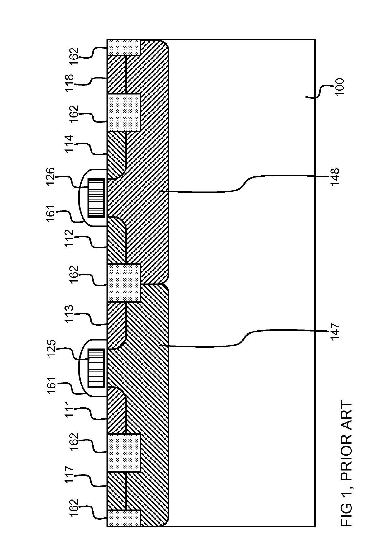
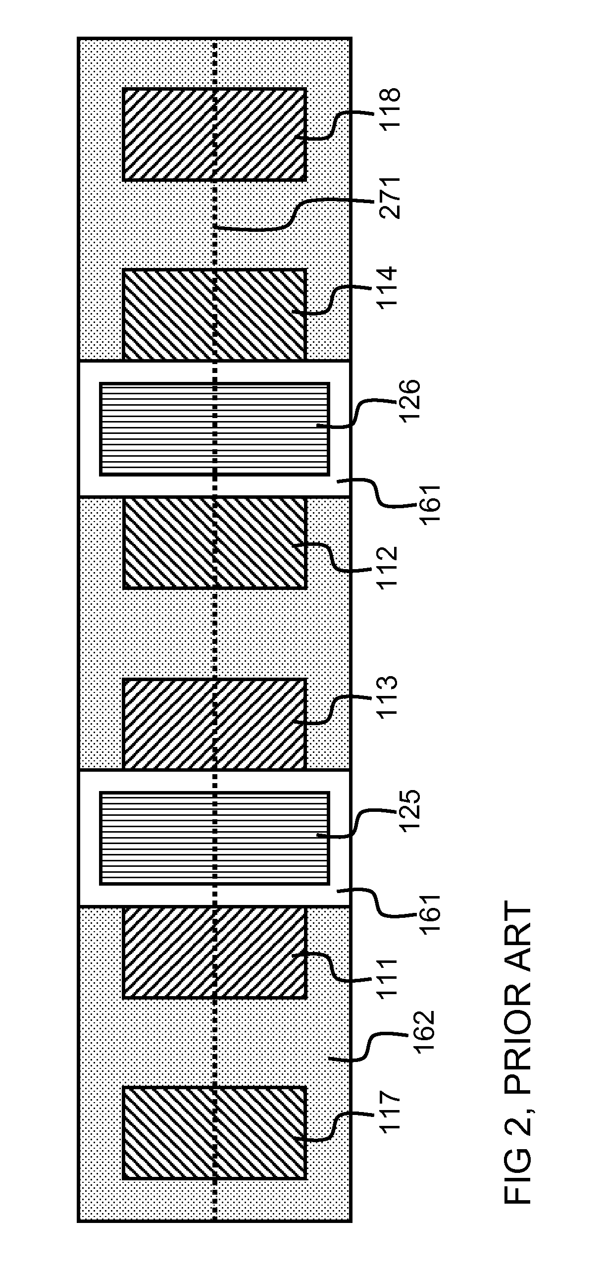
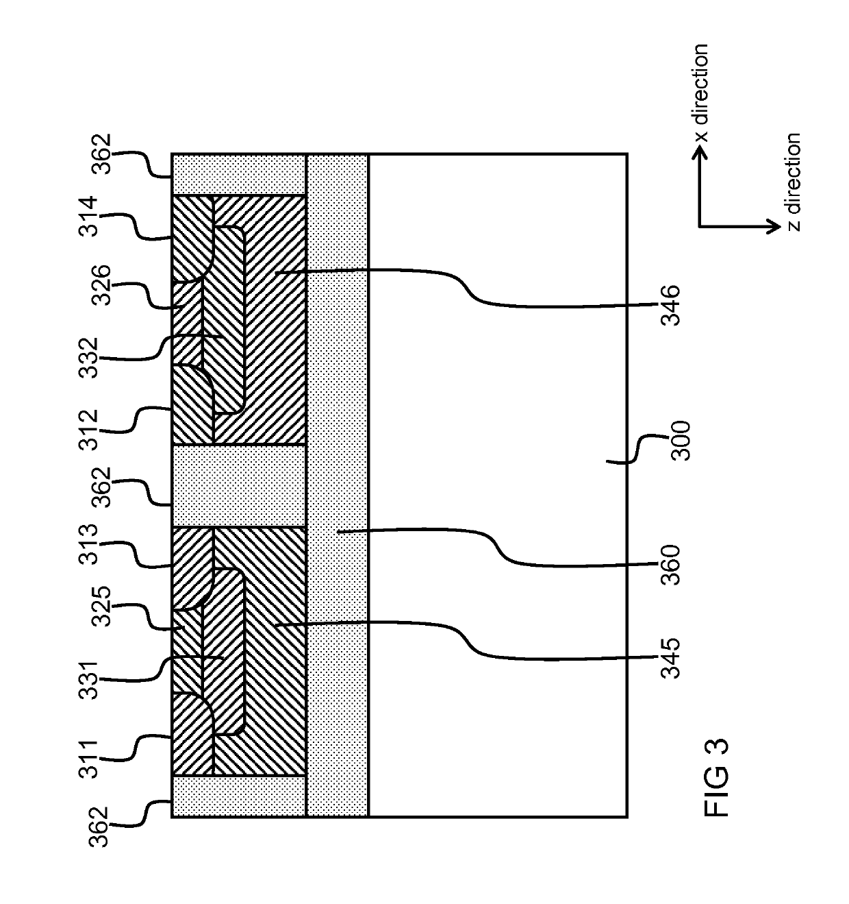
[0048]The specific examples provided in the description given below should not be construed as limiting the scope and / or the applicability of the appended claims. Lists and groups of examples provided in the description given below are not exhaustive unless otherwise explicitly stated.

[0049]As already previously said, in this text the term complementary binary logic refers to a logic circuitry comprising a set of logic elements that correspond either to semiconductor logic elements or to complementary semiconductor logic elements each of them having an input and an output.

During a steady state in the complementary binary logic circuitry[0050]the potential at an input or at an output can have only two different values which are referred to as logic potentials, and[0051]there are no conductive paths between the nodes in the set of semiconductor logic elements that are at different potentials enabling thus low steady state power consumption.

In addition, it is only possible in complemen...


PUM


Abstract

Disclosed is a semiconductor logic element having a field effect transistor of the first conductivity type and a field effect transistor of the second conductivity type. A gate of the first FET is an input of the semiconductor logic element, a drain of the second FET is referred to as the output of the semiconductor logic element and a source of the second FET is the source of the semiconductor logic element. By applying applicable potentials to the terminals of the field effect transistors it is possible to influence the state of the output of the logic element. Also disclosed are different kinds of logic circuitries with the described logic element.

Description

FIELD OF THE INVENTION[0001]The invention relates to semiconductor solutions. More specifically, the invention relates to semiconductor logic elements replacing, at least partly, traditional semiconductor logic elements in complementary binary logic.BACKGROUND OF THE INVENTION[0002]For sake of clarity of the disclosure the following remarks are done. In this text the term complementary binary logic refers to a logic circuitry comprising a set of logic elements that correspond either to semiconductor logic elements or to complementary semiconductor logic elements each of them having an input and an output. During a steady state in the complementary binary logic circuitry[0003]the potential at an input or at an output can have only two different values which are referred to as logic potentials, and[0004]there are no conductive paths between the nodes in the set of semiconductor logic elements that are at different potentials enabling thus low steady state power consumption.[0005]In ad...

Claims


Application Information

Patent Timeline
IPC IPC(8): H01L27/092H01L27/02H01L27/098H01L27/12H03K19/003H03K19/20H01L21/8238H03K19/0952
CPCH01L27/092H01L27/0207H01L27/098H01L27/1203H03K19/003H03K19/20H01L21/823807H03K19/0952H01L27/085H03K19/094
Inventor AUROLA, ARTTO
Owner HYPERION SEMICON OY
Features
  • Generate Ideas
  • Intellectual Property
  • Life Sciences
  • Materials
  • Tech Scout
  • Unparalleled Data Quality
  • Higher Quality Content
  • 60% Fewer Hallucinations
Learn More