
OLED display device

a display device and flexible technology, applied in the direction of semiconductor devices, basic electric elements, electrical apparatus, etc., can solve the problems of unfavorable narrow frame design, uncontrollable boundary of organic layer, relative high fluidity, etc., to facilitate the development of narrow frame design and prevent film from breaking

Inactive Publication Date: 2019-08-29
WUHAN CHINA STAR OPTOELECTRONICS SEMICON DISPLAY TECH CO LTD
View PDF8 Cites 8 Cited by
  • Summary
  • Abstract
  • Description
  • Claims
  • Application Information

AI Technical Summary

Benefits of technology

The present invention provides an OLED display device that prevents the film from breaking during cutting and ensures a smooth product surface. This is achieved by creating a discontinuity in the outermost inorganic layer to interrupt the mechanical stress generated by cutting. This allows for a narrower frame design and also facilitates the development of advanced materials for OLED display devices.

Problems solved by technology

However, because the organic material is particularly sensitive to external water and oxygen, flexible encapsulating is directly related to the display lifetime of the OLED, which is also one of the bottlenecks that limit the development of OLED.
The organic layer in the encapsulation structure is generally realized by flash evaporation, inkjet printing (IJP), and the like, wherein the IJP method has a shorter encapsulating time and an excellent planarization effect, but the organic layer is coated with a monomer that has a relatively high fluidity such that the boundary of the organic layer cannot be well controlled.
However, the design of the narrow frame is unfavorable, mainly because the outermost inorganic layer is prepared by using the entire surface coating to form a continuously connected film layer, so that the mechanical stress generated by the cutting during the production of the narrow frame will continue to be transmitted.
The edge of the outermost inorganic layer cracks, which affects the surface roughness of the product.

Method used


Image

  • OLED display device

Examples


Embodiment Construction

[0031]Through following to combine figures to describe in detail, the above, the other purposes, the features and benefits of the exemplary embodiment of the present disclosure will become clearer.

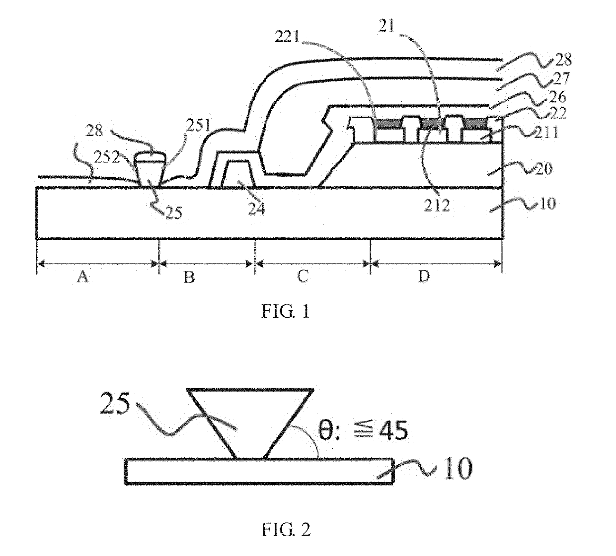
[0032]As shown in FIG. 1, an OLED display device provided in a first embodiment of the present invention includes:

[0033]a base substrate 10;

[0034]a planarization layer 20 disposed on the substrate 10, an outer barrier wall 25, and an inner barrier wall 24 located between the planarization layer 20 and the outer side wall 25; wherein the outer barrier wall 25 is provided with a first side surface 251 facing toward the planarization layer 20 and a second side surface 252 away from the planarization layer 20, and at least one of the first side surface 251 and the second side surface 252 forms an acute angle relationship with the base substrate 10;

[0035]multiple light emitting devices 21 and a pixel defining layer 22 disposed on the planarization layer 20, wherein each light emitting device 21...


PUM


Abstract

An OLED display device is disclosed. The device includes: a base substrate; a planarization layer disposed on the substrate, an outer barrier wall, and an inner barrier wall; multiple light emitting devices and a pixel defining layer disposed on the planarization layer; a first inorganic layer covering the pixel defining layer and each light emitting device, wherein the first inorganic layer is extended to the inner barrier wall and covering the inner barrier wall; an organic layer disposed on the first inorganic layer, and an extending length of the organic layer is less than an extending length of the first inorganic layer; and a second inorganic layer disposed on the organic layer, the first inorganic layer, the outer barrier wall and the base substrate; wherein, the second inorganic layer is in a discontinuous connection state using the outer barrier wall as a breakpoint.

Description

CROSS REFERENCE[0001]This application is a continuing application of PCT Patent Application No. PCT / CN2018 / 080854, entitled “OLED DISPLAY DEVICE”, filed on Mar. 28, 2018, which claims priority to China Patent Application No. 201810162851.4, filed on Feb. 27, 2018, both of which are hereby incorporated in its entireties by reference.FIELD OF THE INVENTION[0002]The present invention relates to a flexible display technology field, and more particularly to an OLED display device.BACKGROUND OF THE INVENTION[0003]The Organic Light-Emitting Diode (OLED) has the advantages of fast response, wide temperature range, self-luminous, and flexible display, and is regarded as a third-generation display technology after CRT, LCD, and LED. With the continuous increasing in market demand, the development and production of flexible OLED has become a hot area for display industry. However, because the organic material is particularly sensitive to external water and oxygen, flexible encapsulating is dir...

Claims


Application Information

Patent Timeline
Patent Type & Authority Applications(United States)
IPC IPC(8): H01L51/52H01L27/32
CPCH01L51/5253H01L51/0097H01L27/3258H01L27/3246H10K59/124H10K59/8731H10K50/844H10K59/122H10K77/111
Inventor HUANG, JINGHSU, HSIANGLUN
Owner WUHAN CHINA STAR OPTOELECTRONICS SEMICON DISPLAY TECH CO LTD
Learn More