Rapid preparation method of high flatness and low damage single crystal silicon carbide substrate

A single crystal silicon carbide and flatness technology, which is applied in semiconductor/solid-state device manufacturing, electrical components, circuits, etc., can solve the problems that the disk surface affects the wafer surface shape, deep scratches, and processing efficiency reduction, so as to improve processing efficiency, Shallow embedding scratches and good surface parameters

Active Publication Date: 2019-03-29
SICC CO LTD
View PDF3 Cites 8 Cited by
  • Summary
  • Abstract
  • Description
  • Claims
  • Application Information

AI Technical Summary

Problems solved by technology

In the next step of chip manufacturing, these unqualified areas will greatly reduce the chip yield, which is the primary factor affecting the chip yield
[0005] Due to the use of sand wire cutting in the prior art, which is a cutting method similar to grinding, the cutting force is very weak, which greatly reduces the processing efficiency; during the grinding process of free abrasives, large particles of free abrasives will cause deep scratches , the next process is difficult to remove
Copper plate and tin plate are single-sided processing methods. Because the plate surface is soft, poor control of the flatness of the plate surface will seriously affect the wafer surface shape (TTV / LTV / BOW / Warp)
[0006] There has always been a contradiction between surface quality and removal rate in traditional alkaline CMP processing: using high-hardness abrasives can increase the removal rate, but it will cause surface damage; using low-hardness abrasives can obtain high-quality surfaces, but the removal rate is very low
If there is a damaged layer on the finally obtained wafer surface, it will have a fatal impact on the application

Method used


Image

  • Rapid preparation method of high flatness and low damage single crystal silicon carbide substrate
  • Rapid preparation method of high flatness and low damage single crystal silicon carbide substrate
  • Rapid preparation method of high flatness and low damage single crystal silicon carbide substrate

Examples


preparation example Construction

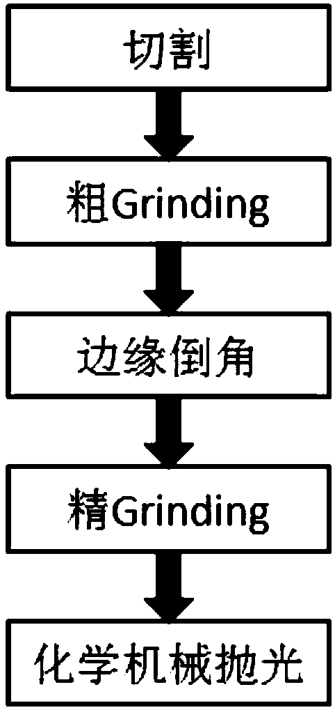
[0047] A method for preparing a high-flatness, low-damage single-crystal silicon carbide substrate, the preparation method comprising:

[0048] Step 1, initial processing: perform initial processing on the single crystal silicon carbide substrate;

[0049] Step 2. Diamond wire cutting: use a diamond wire to cut the monocrystalline silicon carbide initially processed in step 1, wherein the cutting wire tension is 22-40N, the wire running speed is 1200-1800m / min, and the swing angle is 1-10°. Knife speed 5-15mm / h, diamond wire diameter 0.12-0.28mm;

[0050] Step 3, grinding wheel grinding: Install grinding wheels of two meshes in the two stations of the Grinding (grinding) equipment respectively, as rough grinding and fine grinding, and grind the single crystal silicon carbide cut by the diamond wire in step 2, wherein , use 1000-5000-mesh grinding wheel for coarse grinding, speed, feed speed; fine grinding use 20000-30000-mesh grinding wheel, speed 1000-2000rpm, feed speed 0.2...

Embodiment 1

[0053] A method for preparing a high-flatness, low-damage single-crystal silicon carbide substrate with a diameter of 100 mm, the preparation method comprising:

[0054] Step 1, initial processing: perform initial processing on the single crystal silicon carbide substrate;

[0055] Step 2. Diamond wire cutting: use a diamond wire to cut the monocrystalline silicon carbide initially processed in step 1, wherein the cutting wire tension is 22N, the wire running speed is 1200m / min, the swing angle is 5°, and the feed speed is 5mm / h. Diamond wire diameter 0.12mm;

[0056] Step 3, grinding wheel grinding: Install grinding wheels of two meshes in the two stations of the Grinding (grinding) equipment respectively, as rough grinding and fine grinding, and grind the single crystal silicon carbide cut by the diamond wire in step 2, wherein , use 1000-mesh grinding wheel for coarse grinding, speed, feed speed; use 20000-mesh grinding wheel for fine grinding, speed 1000rpm, feed speed 0....

Embodiment 2

[0062] A method for preparing a high-flatness, low-damage single-crystal silicon carbide substrate with a diameter of 100 mm, the preparation method comprising:

[0063] Step 1, initial processing: perform initial processing on the single crystal silicon carbide substrate;

[0064] Step 2. Diamond wire cutting: use a diamond wire to cut the monocrystalline silicon carbide initially processed in step 1, wherein the cutting wire tension is 40N, the wire running speed is 1800m / min, the swing angle is 10°, and the feed speed is 15mm / h. Diamond wire diameter 0.28mm;

[0065] Step 3, grinding wheel grinding: Install grinding wheels of two meshes in the two stations of the Grinding (grinding) equipment respectively, as rough grinding and fine grinding, and grind the single crystal silicon carbide cut by the diamond wire in step 2, wherein , rough grinding uses 5000 mesh grinding wheel, speed, feed speed; fine grinding uses 30000 mesh grinding wheel, speed 2000rpm, feed speed 1um / s; ...


PUM

PropertyMeasurementUnit
particle diameteraaaaaaaaaa
diameteraaaaaaaaaa
diameteraaaaaaaaaa

Abstract

The invention provides a rapid preparation method of a high flatness and low damage single crystal silicon carbide substrate. The method is characterized by comprising steps that fully-solidified abrasive treatment of the single crystal silicon carbide is performed, chemical mechanical polishing treatment is then performed, the high-flatness and low-damage single crystal silicon carbide substrateis obtained, solidified abrasive treatment includes line cutting and grinding wheel grinding, abrasive particles are consolidated on cutting lines, and the abrasive particles are consolidated on a grinding wheel. The method is advantaged in that surface roughness, a scratch die ratio, a pit ratio and bump of the prepared single crystal silicon carbide substrate are relatively low, surface data isgood, thickness deviation is small, curvature is small, and warpage is small.

Description

technical field [0001] The invention relates to the technical field of crystal material processing, in particular to a rapid preparation method of a high flatness and low damage single crystal silicon carbide substrate. Background technique [0002] Single crystal silicon carbide is one of the most important third-generation semiconductor materials. Because of its excellent properties such as large band gap, high saturated electron mobility, strong breakdown field, and high thermal conductivity, it is widely used in power electronics, radio frequency devices, and optoelectronics. Devices and other fields have a wide range of application prospects. [0003] At present, the growth method of PVT (Physical Vapor Deposition) is mostly used for commercial single-crystal silicon carbide, and then through end-face processing, multi-wire cutting, grinding, mechanical polishing, chemical-mechanical polishing, cleaning and packaging, a ready-to-use silicon carbide substrate is formed. ...

Claims


Application Information

Patent Timeline
Patent Type & Authority Applications(China)
IPC IPC(8): H01L21/306
CPCH01L21/30625
Inventor 梁庆瑞王含冠王瑞时文灵
Owner SICC CO LTD
Why Eureka
Try Eureka