

Chemical vapor deposition wafer carrier with thermal cover
- Summary
- Abstract
- Description
- Claims
- Application Information
AI Technical Summary
Benefits of technology
Problems solved by technology
Method used
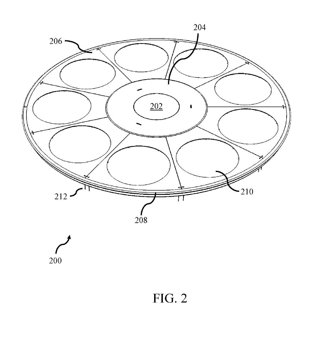
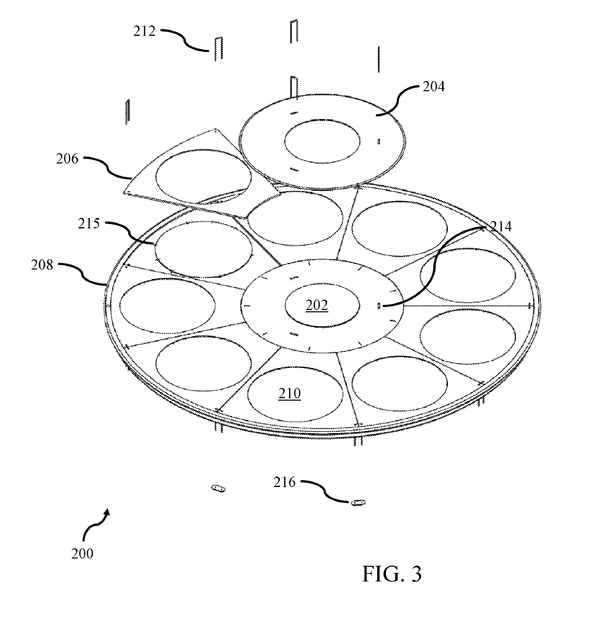
Image

Examples
Embodiment Construction
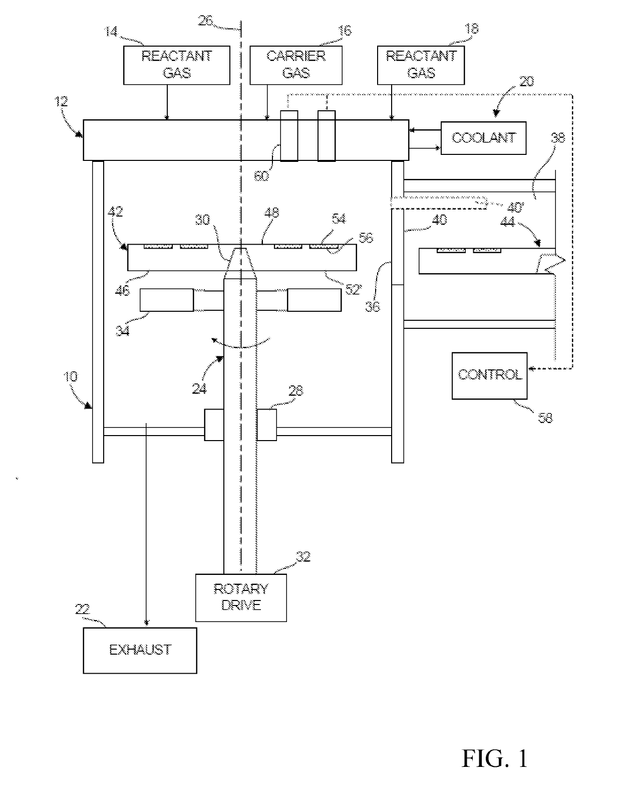
[0037]FIG. 1 illustrates a chemical vapor deposition apparatus in accordance with one embodiment of the invention. The embodiment shown in FIG. 1 is just one version of a chemical vapor deposition system, and others, such as the PROPEL™ system that is sold by VEECO®, described in more detail in U.S. Patent Application Pub. No. 2015 / 0075431, which is incorporated by reference herein in its entirety.
[0038]As shown in FIG. 1, reaction chamber 10 defines a process environment space. Gas distribution device 12 is arranged at one end of the chamber. The end having gas distribution device 12 is referred to herein as the “top” end of reaction chamber 10. This end of the chamber typically, but not necessarily, is disposed at the top of the chamber in the normal gravitational frame of reference. Thus, the downward direction as used herein refers to the direction away from gas distribution device 12; whereas the upward direction refers to the direction within the chamber, toward gas distributi...
PUM
| Property | Measurement | Unit |
|---|---|---|
| Thickness | aaaaa | aaaaa |
| Diameter | aaaaa | aaaaa |
| Structure | aaaaa | aaaaa |
Abstract
Description
Claims
Application Information