TFT pixel threshold voltage compensation circuit with light-emitting device initialization

Active Publication Date: 2019-10-03
SHARP KK
View PDF1 Cites 7 Cited by
  • Summary
  • Abstract
  • Description
  • Claims
  • Application Information

AI Technical Summary

Benefits of technology

[0009]The present invention relates to pixel circuits that are capable of compensating the threshold voltage variations of the drive transistor with fewer transistors than in conventional configurations, with additionally (1) reducing or eliminating the possib

Problems solved by technology

Therefore, pixels in a display may not exhibit uniform brightness for a given VDAT value.
A first problem with this is that it may affect the true black state.
A second problem is memory effects from the previous frame data.
If the programmed current is a low current, it could take a significant time to refresh the anode to the programmed value.
There are significant drawbacks with such configuration and method.
This may cause an instance of high luminance light, which would prevent a pixel from ever having a true black state.
Other approaches to address the above problems have proven deficient.
This approach, however, could cause a leakage current durin

Method used


Image

  • TFT pixel threshold voltage compensation circuit with light-emitting device initialization
  • TFT pixel threshold voltage compensation circuit with light-emitting device initialization
  • TFT pixel threshold voltage compensation circuit with light-emitting device initialization

Examples


first embodiment

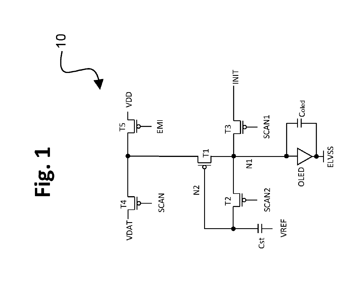
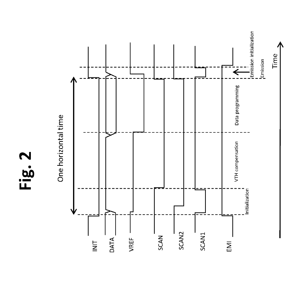
[0040]In this first embodiment, during the first initialization phase memory effects from residual voltages from the previous frame are essentially eliminated. At the outset, an EMI signal level is set to a high voltage value, causing transistor T5 to be off. Consequently, the source of the drive transistor T1 is disconnected from a second power supply, VDD. In addition, an initialization voltage signal (INIT) is changed from a high reference voltage level, INIT_H, to a low reference voltage level INIT_L. Preferably, INIT_H is similar to the voltage at the anode of the OLED that results in the lowest light emission from the OLED during the emission phase for typical operation of the display. Accordingly, INIT_L, being lower than INIT_H, has a value that may reverse bias the OLED, i.e., INIT_L may be is less than ELVSS. The value of INIT_L also should be set so as not to cause significant degradation of the OLED.

[0041]Further during the first initialization phase, a SCAN1 signal leve...

second embodiment

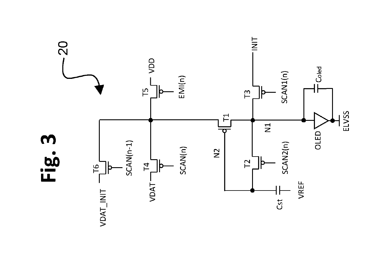
[0086]The advantages may be achieved using as few as only five transistors and one storage capacitor, thereby providing a smaller circuit as compared to conventional configurations. By the addition of a sixth transistor in the second embodiment, although the circuit size is increased, the circuit size still is small as compared to conventional configurations, and a significantly shortened horizontal time is achieved.

[0087]The various embodiments have been described in connection with OLEDs as the display light-emitting device. The circuit configurations, however, are not limited to any particular display technology. For example, the circuit configurations also may also be used for micro LED displays, quantum dot LED displays, or any other device which emits light in response to an applied electrical bias. A micro LED, for example, is a semiconductor device containing a p-type region, an n-type region and a light emission region, for example formed on a substrate and divided into ind...


PUM


Abstract

A pixel circuit for a display device includes a drive transistor configured to control an amount of current to a light-emitting device depending upon a voltage applied to a gate of the drive transistor; a second transistor connected to the gate of the drive transistor and a second terminal of the drive transistor such that, when the second transistor is in an on state the drive transistor becomes diode-connected such that the gate and a second terminal of the drive transistor are connected through the second transistor; a light-emitting device that is connected at a first node to the second terminal of the drive transistor and at a second node to a first voltage supply; a third transistor that is connected between an initialization voltage supply and the first node of the light-emitting device, wherein a node N1 is a connection of the second terminal of the drive transistor, the first node of the light-emitting device, and the third transistor; and at least one capacitor having a first plate that is connected to the gate of the drive transistor and a second plate that is connectable to a reference voltage supply. The pixel circuit is operable in an initialization phase to initialize circuit voltages, in a compensation phase to compensate for variations in drive transistor properties, in a programming phase to program a greyscale value to the pixel circuit, and in an emission phase in which the light-emitting device emits light corresponding to the greyscale value.

Description

TECHNICAL FIELD[0001]The present invention relates to design and operation of electronic circuits for delivering electrical current to an element in a display device, such as for example to an organic light-emitting diode (OLED) in the pixel of an active matrix OLED (AMOLED) display device.BACKGROUND ART[0002]Organic light-emitting diodes (OLED) generate light by re-combination of electrons and holes, and emit light when a bias is applied between the anode and cathode such that an electrical current passes between them. The brightness of the light is related to the amount of the current. If there is no current, there will be no light emission, so OLED technology is a type of technology capable of absolute blacks and achieving almost “infinite” contrast ratio between pixels when used in display applications.[0003]Several approaches are taught in the prior art for pixel thin film transistor (TFT) circuits to deliver current to an element of a display device, such as for example an org...

Claims


Application Information

Patent Timeline
IPC IPC(8): G09G3/3233H01L27/32
CPCG09G2320/043G09G2310/0243G09G2300/0861G09G3/3233H01L27/3262H01L27/3265H01L27/3248G09G3/3258G09G3/3291G09G3/32G09G2300/0866G09G2320/0233G09G2300/0465G09G2300/0819G09G2300/0842G09G2310/0251G09G2310/06G09G2330/021G09G2320/045G09G2320/0238H10K59/123H10K59/1213H10K59/1216
Inventor LU, TONGBROWNLOW, MICHAEL JAMESSMEETON, TIM MICHAEL
Owner SHARP KK
Why Eureka
Try Eureka