Method of forming an electrode on a substrate and a semiconductor device structure including an electrode

a technology of semiconductor devices and substrates, applied in the direction of coatings, transistors, basic electric elements, etc., can solve the problems of unwanted thermal diffusion of metal species, undesirable diffusion, formation of unwanted materials,

Active Publication Date: 2019-10-03
ASM IP HLDG BV
View PDF11 Cites 258 Cited by
  • Summary
  • Abstract
  • Description
  • Claims
  • Application Information

AI Technical Summary

Problems solved by technology

In particular semiconductor fabrication processes, high temperature deposition of metal-containing films may result in, unwanted thermal diffusion of metal species into adjacent dielectric materials, undesirable diffusion of dopant species in transistor structures, and the formation of unwanted materials.
However, a reduction in the deposition temperature of metal-containing films, such as, for example, titanium nitride films, may have a detrimental effect on the quality of the deposited film.

Method used


Image

  • Method of forming an electrode on a substrate and a semiconductor device structure including an electrode
  • Method of forming an electrode on a substrate and a semiconductor device structure including an electrode
  • Method of forming an electrode on a substrate and a semiconductor device structure including an electrode

Examples


Embodiment Construction

[0021]Although certain embodiments and examples are disclosed below, it will be understood by those in the art that the invention extends beyond the specifically disclosed embodiments and / or uses of the invention and obvious modifications and equivalents thereof. Thus, it is intended that the scope of the invention disclosed should not be limited by the particular disclosed embodiments described below.

[0022]The illustrations presented herein are not meant to be actual views of any particular material, structure, or device, but are merely idealized representations that are used to describe embodiments of the disclosure.

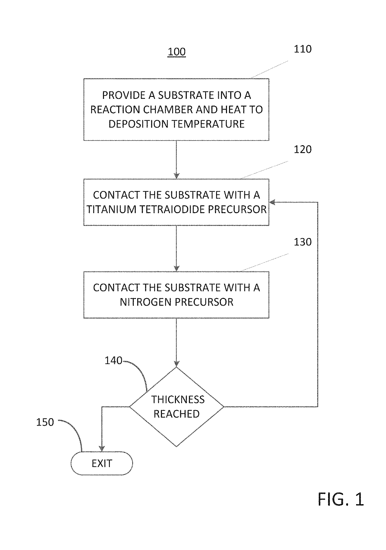
[0023]As used herein, the term “cyclic deposition” may refer to the sequential introduction of precursors (reactants) into a reaction chamber to deposit a film over a substrate and includes deposition techniques, such as atomic layer deposition and cyclical chemical vapor deposition.

[0024]As used herein, the term “cyclical chemical vapor deposition” may refer to any pr...


PUM

PropertyMeasurementUnit
temperatureaaaaaaaaaa
Raaaaaaaaaaa
densityaaaaaaaaaa

Abstract

A method of forming an electrode on a substrate is disclosed. The method may include: contacting the substrate with a first vapor phase reactant comprising a titanium tetraiodide (TiI4) precursor; contacting the substrate with a second vapor phase reactant comprising a nitrogen precursor; and depositing a titanium nitride layer over a surface of the substrate thereby forming the electrode; wherein the titanium nitride layer has an electrical resistivity of less than 400 μΩ-cm. Related semiconductor device structures including a titanium nitride electrode deposited by the methods of the disclosure are also provided.

Description

CROSS-REFERENCE TO RELATED PATENT APPLICATION[0001]The present claims the benefit of U.S. Provisional Patent Application No. 62 / 648,832, filed on Mar. 27, 2018 and entitled “METHOD OF FORMING AN ELECTRODE ON A SUBSTRATE AND A SEMICONDUCTOR DEVICE STRUCTURE INCLUDING AN ELECTRODE,” the disclosure of which is incorporated herein by reference.FIELD OF INVENTION[0002]The present disclosure relates generally to methods for forming an electrode on a substrate and particularly methods for a forming a titanium nitride electrode on a partially fabricated semiconductor device structure. The present disclosure also generally relates to a semiconductor device structure and particularly a semiconductor device structure including a titanium nitride electrode.BACKGROUND OF THE DISCLOSURE[0003]In the field of semiconductor device fabrication, the trend is towards a reduction in the deposition temperature of metal-containing films, such as, for example, pure metals, metal nitrides, metal carbides, a...

Claims


Application Information

Patent Timeline
Patent Type & Authority Applications(United States)
IPC IPC(8): H01L21/28H01L21/02H01L21/285
CPCH01L29/4966H01L28/60H01L21/0228H01L21/02186H01L21/02205H01L21/285H01L21/28088H01L27/1085H01L21/823842H01L21/32051H01L21/28562H01L21/76877H01L23/53261C23C16/34C23C16/45553H01L21/28026H01L21/28194H01L21/324H01L27/092H01L2924/04941H10B12/00H10B12/03
Inventor MOUSA, MOATAZ BELLAHHSU, PENG-FUJOHNSON, WARDRAISANEN, PETRI
Owner ASM IP HLDG BV
Why Eureka
Try Eureka