Systems and methods for releveled bump planes for chiplets

a bump plane and chiplet technology, applied in the direction of electrical apparatus, semiconductor devices, semiconductor/solid-state device details, etc., can solve the problems of increasing the complexity of the overall the increase of the complexity of the design of the ic and other microscale structures, and the increase of the use of advanced nodes

Active Publication Date: 2019-12-26
ADEIA SEMICON INC
View PDF5 Cites 6 Cited by
  • Summary
  • Abstract
  • Description
  • Claims
  • Application Information

AI Technical Summary

Benefits of technology

[0018]In still other embodiments, the first photo resist layer is patterned and exposed in such a manner that the exposed openings on the chip level are larger than the openings on the chiplet level, such that as the plating of the posts in the plurality of openings results in larger posts on the chip level than on the chiplet level such that the plating results in a single level that may not require additional releveling.

Problems solved by technology

These demands on the industry have led to the increased complexity of the design of the ICs and other microscale structures.
The ever-increasing demand for smaller, faster, better components has led to the development of new methods of manufacture like the 3-D stacking that also present other issues as the overall design of the IC becomes more and more complex.
The increased complexity of design also included the increased use of more advanced nodes and blocks that are incorporated into the overall IC design.
These advanced nodes also pose potential issues in the overall function and structure of the IC because of their complexity and size thus driving a need to improve on how advanced portions of an IC are incorporated into the overall design and function of the microscale structure.

Method used


Image

  • Systems and methods for releveled bump planes for chiplets
  • Systems and methods for releveled bump planes for chiplets
  • Systems and methods for releveled bump planes for chiplets

Examples


Embodiment Construction

[0041]The present disclosure may be understood by reference to the following detailed description, taken in conjunction with the drawings as described below. It is noted that, for purposes of illustrative clarity, certain elements in various drawings may not be drawn to scale.

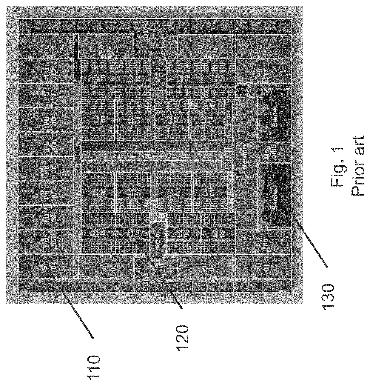
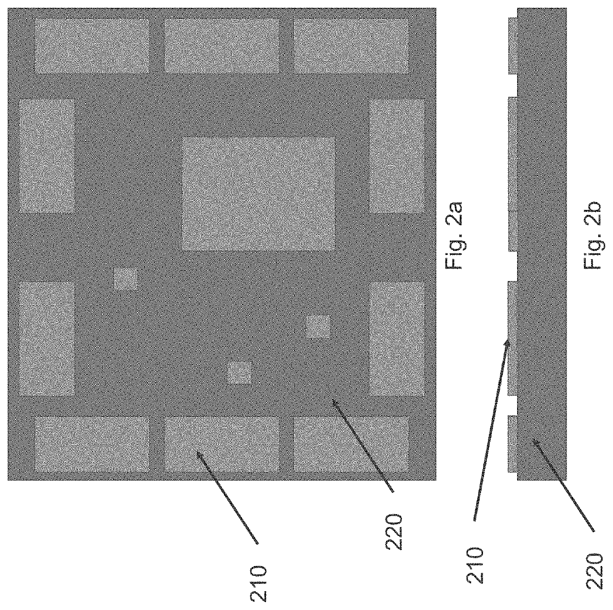
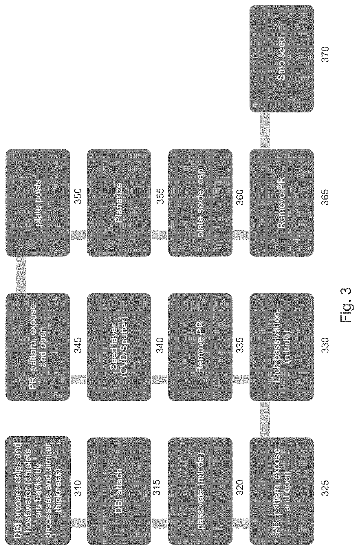
[0042]The configuration of various levels of a stacked integrated circuit including methods for producing such are described herein. In accordance with many embodiments chiplets are bonded to a chip with DBI technology having fine pitch interconnects and TSVs wherein a bump plane is created and releveled creating a single level bump plane for additional boding of layers.

[0043]Integrated circuit design generally deals with the creation of electrical components and the design and placement of such components onto a platform such as a silicon wafer. The design and layout of the electrical components is performed in such a way as to create functional blocks designed to perform certain processes of the integrated ci...


PUM


Abstract

An integrated circuit and a method for designing an IC wherein the base or host chip is bonded to smaller chiplets via DBI technology. The bonding of chip to chiplet creates an uneven or multi-level surface of the overall chip requiring a releveling for future bonding. The uneven surface is built up with plating of bumps and subsequently releveled with various methods including planarization.

Description

FIELD OF THE INVENTION[0001]The following description relates to the design of microelectronic structures. More specifically it relates to the reconfiguration of the bump plane on chiplets when bonding multiple die.BACKGROUND[0002]Microelectronics typically involve the use of thin semiconductor materials such as silicon wafers that may be formed into individual units or dies. Such elements are often used in integrated circuits (ICs) that may be subsequently installed onto printed circuit boards (PCBs). The field of Microelectronics has rapidly expanded over the last few decades with a demand for greater storage or memory capacity and decreased size. Additionally, cost reduction is a continual concern that greatly influences the development of new microelectronic technologies and procedures. These demands on the industry have led to the increased complexity of the design of the ICs and other microscale structures.[0003]The demand for consumer products and applications for higher perf...

Claims


Application Information

Patent Timeline
Patent Type & Authority Applications(United States)
IPC IPC(8): H01L25/065H01L23/00
CPCH01L2225/06517H01L2225/06544H01L24/11H01L2224/11464H01L2224/13005H01L2224/119H01L25/0652H01L2224/08146H01L2225/06555H01L24/08H01L2224/92244H01L2224/73267H01L2224/04105H01L2224/12105H01L23/5389H01L2224/08225H01L2224/08145H01L25/0655H01L2225/06524H01L2225/06513H01L2225/06541H01L25/50H01L2224/9212H01L2224/9222H01L2224/9202H01L24/92H01L24/03H01L2224/0345H01L2224/03452H01L2224/1147H01L2224/03464H01L2224/1146H01L2224/1184H01L2224/11845H01L2224/1183H01L2224/1163H01L2224/03912H01L2224/0347H01L2224/11903H01L2224/11474H01L24/13H01L24/14H01L2224/1403H01L2224/13082H01L2224/16145H01L2224/05647H01L2224/05686H01L2224/05576H01L2224/80948H01L2224/80895H01L2224/80896H01L2924/3651H01L24/19H01L24/20H01L2224/13022H01L2224/1191H01L2224/1148H01L24/05H01L24/16H01L24/80H01L2924/181H01L21/56H01L23/3185H01L23/3171H01L2924/381H01L2224/131H01L2224/80H01L2224/03H01L2224/11H01L2924/00014H01L2924/00012H01L2224/034H01L2224/0361H01L2224/81H01L2924/014
Inventor DELACRUZ, JAVIER A.HABA, BELGACEMUZOH, CYPRIAN EMEKAKATKAR, RAJESHMOHAMMED, ILYAS
Owner ADEIA SEMICON INC
Why Eureka
Try Eureka