Light emitting device, display device, and LED display device

a technology of led display device and light emitting device, which is applied in the direction of instruments, static indicating devices, etc., can solve the problems of chromaticity change depending on the current value, difficulty in implementing an approach to driving leds, and difficulty in performing control to obtain brightness with desired accuracy. , to achieve the effect of reducing the number of lines for driving leds, and reducing the occurrence of display defects

Active Publication Date: 2020-01-02
SHARP KK
View PDF1 Cites 8 Cited by
  • Summary
  • Abstract
  • Description
  • Claims
  • Application Information

AI Technical Summary

Benefits of technology

[0036]According to the above configuration, one or more LEDs that constitute each of the LED units are driven by active matrix-type driving. Specifically, signal lines for supplying the data voltage to the LEDs are provided for respective columns, and the LEDs are driven row by row. Therefore, there is no possibility that the number of lines for driving the LEDs becomes enormous. Further, an entire part of one frame period is taken as the display period. Moreover, the LED drive circuit turns on the LEDs for a period of a length depending on the data voltage held in the data voltage holding unit. Specifically, brightness of the LEDs is controlled by the PWM dimming control. Therefore, it is possible to reduce occurrence of display defects such as variation in brightness. Furthermore, the lighting period control operation is performed more than once for each frame period. This makes the lighting cycle of the LEDs shorter, and prevents flicker from occurring. As described above, it is possible to realize a light emitting device capable of controlling a large number of LEDs independently without causing display defects such as variation in brightness and flicker.(2) Moreover, light emitting devices according to several embodiments of the present invention are each a light emitting device including the configuration of above (1), wherein

Problems solved by technology

However, in recent years, an LED (light-emitting diode) has become widely employed due to low power consumption and facilitation of brightness control.
However, according to the analog dimming control method, as relationship between the current flowing through the LED and the brightness of the LED is non-linear, it is difficult to perform control to obtain brightness with desired accuracy.
In addition, the analog dimming control method poses another problem that chromaticity may change depending on the current value.
In this regard, it is difficult to implement an approach of driving LEDs for each area using the configuration shown in FIG. 12 due to reasons such as an enormous number of lines being required.
Considering the above circumstances, if division of a display region into multiple areas is promoted by employment of microscopic LEDs, a number of sub-frame periods that constitute one frame period significantly increases, which will make it difficult to drive LEDs.
However, if a circuit of a configuration as shown in FIG. 17 is used, since the analog dimming control method is employed as the dimming control method for the LEDs, problems such as chromaticity change due to brightness of light emission and brightness variation among pixels due to variation in transistor characteristics may easily occur.
However, applying the approach described in Japanese Laid-Open Patent Publication No. 2002-297097 to driving of the LEDs included in the backlight of the liquid crystal display device or the like and driving of the LEDs constituting the LED display device leads to problems stated below.
However, according to the approach of the first practical example described in Japanese Laid-Open Patent Publication No. 2002-297097, the display period is relatively a short period of time as described above, and therefore it is not possible to obtain sufficient brightness.
Further, all the LEDs emit light at once at a frame frequency of an image, and this causes flicker.
The same problem occurs in the case of the LED display device, because the LED display device is required to obtain high brightness since it is often used outdoors.
Therefore, applying the approach of the second practical example to driving of the LEDs included in the backlight causes flicker.
When the number of times of scanning the scanning lines increases in this manner, the length of the select period becomes short, and thus writing a desired voltage to the capacitor becomes difficult.
In other words, it is difficult to cause the LEDs to emit light with desired brightness.

Method used


Image

  • Light emitting device, display device, and LED display device
  • Light emitting device, display device, and LED display device
  • Light emitting device, display device, and LED display device

Examples


first embodiment

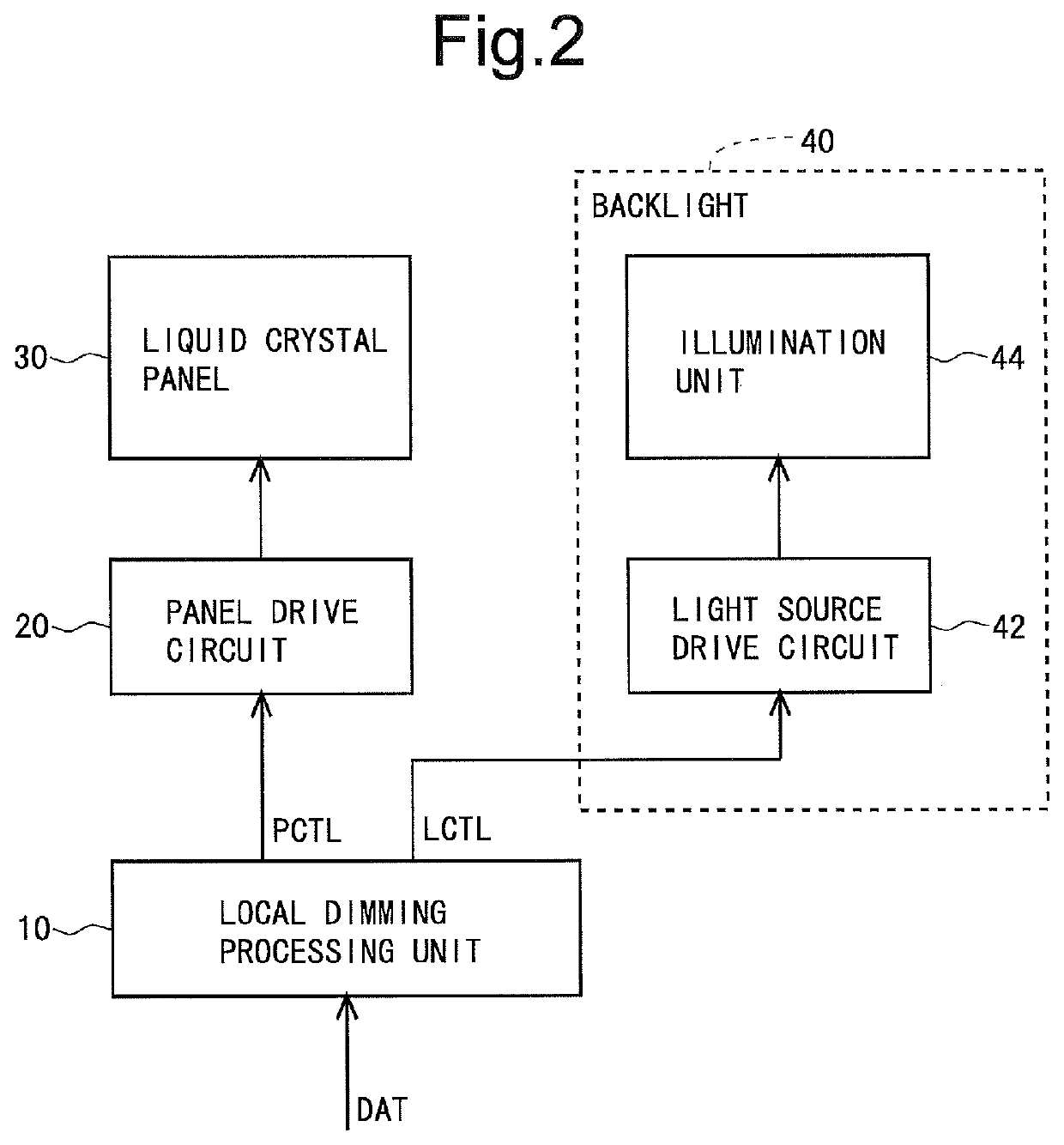
[0120]FIG. 2 is a block diagram showing an entire configuration of a liquid crystal display device according to the first embodiment. The liquid crystal display device is constituted by a local dimming processing unit 10, a panel drive circuit 20, a liquid crystal panel 30, and a backlight (light emitting device) 40. The liquid crystal panel 30 is configured by two opposing glass substrates, and includes a display unit for displaying an image. The backlight 40 is provided on a back surface of the liquid crystal panel 30. The backlight 40 includes a light source drive circuit 42 and an illumination unit 44. The illumination unit 44 includes LED units (each of the LED units is constituted by one or more LEDs) and LED drive circuits which are mounted on a substrate (LED substrate) and will be described later. The local dimming processing unit 10, the panel drive circuit 20, and the light source drive circuit 42 are typically provided on different substrates.

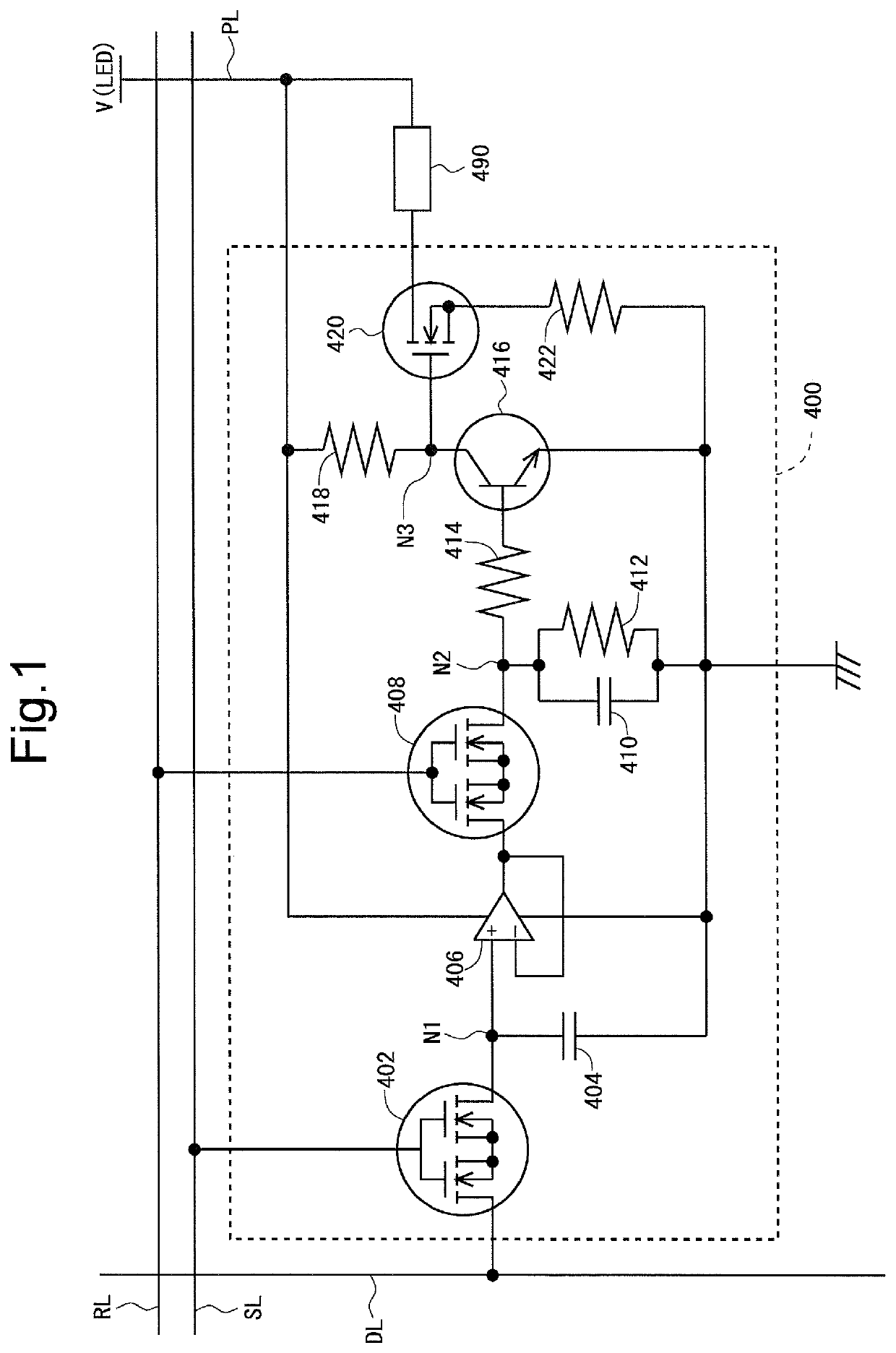
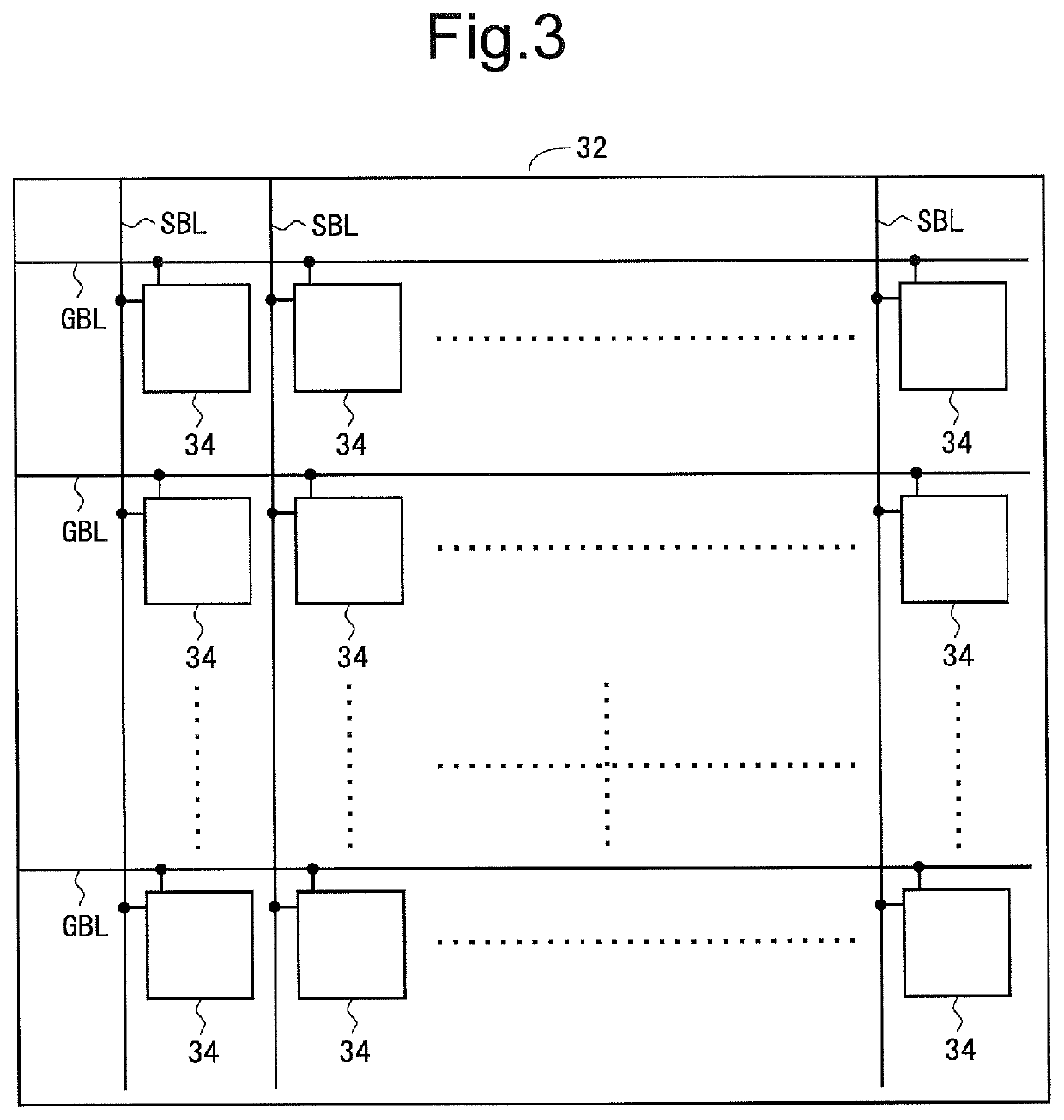
[0121]A display unit 32 in t...

second embodiments

[0155]In a case in which microscopic LEDs such as mini LEDs and micro LEDs are employed for the light source of the backlight, a size of am area as a driving unit for local dimming becomes extremely small. In this case, regarding the LED substrate, it is often difficult to secure region for placing the components such as field-effect transistors (FETs) that constitute the LED drive circuit 400 described above. Therefore, as the second embodiment, an example in which the LED drive circuit 400 and lines such as the scanning lines SL and the like are stacked on the LED substrate will be described.

[0156]As a material of the LED substrate, glass or plastic may be employed. The LED drive circuit 400 and lines such as the scanning lines SL and the like are stacked on the LED substrate. On one surface facing the liquid crystal panel 30 out of surfaces of such a LED substrate, the LEDs are mounted by chip bonding.

[0157]It should be noted that an overall configuration and a schematic configur...

third embodiment

[0167]FIG. 9 is a block diagram showing an entire configuration of a LED display device according to the third embodiment. The LED display device is a display device using LEDs as pixels. As shown in FIG. 9, the LED display device is configured by a video signal processing unit 60, a light source drive circuit 62, and a display unit 64. It should be noted that the display unit 64 in this embodiment corresponds to the illumination unit 44 in the first embodiment (see FIG. 2). Specifically, the display unit 64 is constituted by the LED units and the LED drive circuits which are provided on the substrate (LED substrate). The video signal processing unit 60 and the light source drive circuit 62 are typically disposed on different substrates.

[0168]The video signal processing unit 60 receives the image data DAT transmitted from outside, and outputs the brightness control signal LCTL for controlling an operation of the light source drive circuit 62. Here, the brightness control signal LCTL...


PUM

PropertyMeasurementUnit
brightnessaaaaaaaaaa
lighting frequencyaaaaaaaaaa

Abstract

A plurality of LED drive circuits are provided so as to correspond one-to-one with plurality of LED units arranged in matrix. In the LED drive circuit, a data voltage is written to a memory capacitor in a charge period that appears every one frame period, in the LED drive circuit, the reset control transistor is turned on and off more than once after a time point at which the charge period ends until a time point at which the next charge period starts, so that a lighting enable period in which a lighting period control operation is performed is provided more than once every one frame period.

Description

CROSS REFERENCE TO RELATED APPLICATIONS[0001]This application claims priority to U.S. Provisional Patent Application No. 62 / 690,668, entitled “LIGHT EMITTING DEVICE, DISPLAY DEVICE, AND LED DISPLAY DEVICE”, filed on Jun. 27, 2018, the content of which is incorporated herein by reference.BACKGROUND OF THE INVENTION1. Field of the Invention[0002]The disclosure herein relates to a light emitting device employing LEDs as light sources, a display device using the light emitting device for backlight, and an LED display device constituted by the light emitting device.2. Description of Related Art[0003]A transmissive type liquid crystal display device requires, in order to display images, backlight that emits light to a display unit (liquid crystal panel) from its back surface. Conventionally, as a light source of the backlight, a cold-cathode tube referred to as a CCFL has been widely used. However, in recent years, an LED (light-emitting diode) has become widely employed due to low power ...

Claims


Application Information

Patent Timeline
Patent Type & Authority Applications(United States)
IPC IPC(8): G09G3/3233G09G3/3258G09G3/20
CPCG09G2300/0833G09G2330/021G09G3/2022G09G3/3233G09G2300/0842G09G3/3258G09G3/3406G09G3/32G09G3/3426G09G2310/0262
Inventor MIYATA, HIDEKAZUYAMAGUCHI, NORIAKI
Owner SHARP KK
Why Eureka
Try Eureka