Gate drive circuit

a drive circuit and gate technology, applied in the direction of electronic switching, pulse technique, climate sustainability, etc., can solve the problems of failure of switching elements and additional problems of switching elements, and achieve the effect of not increasing switching losses

Active Publication Date: 2020-01-16
DENSO CORP
View PDF2 Cites 13 Cited by
  • Summary
  • Abstract
  • Description
  • Claims
  • Application Information

AI Technical Summary

Benefits of technology

[0004]The present disclosure describes a gate drive circuit for driving a switching element that can suppress surge voltages without increasing switching losses in the switching element.

Problems solved by technology

In gate drive circuits that drive the gates of switching elements such as insulated-gate bipolar transistors (IGBTs) or metal-oxide-semiconductor field-effect transistors (MOSFETs), surge voltages exceeding the breakdown voltage of the switching element may cause failures in the switching element.
The suppression effects by gate drive circuits to mitigate excessive surge voltages may create additional issues in the switching elements.

Method used


Image

  • Gate drive circuit
  • Gate drive circuit
  • Gate drive circuit

Examples


first embodiment

[0026]The first embodiment of the present disclosure is described with reference to FIGS. 1-4.

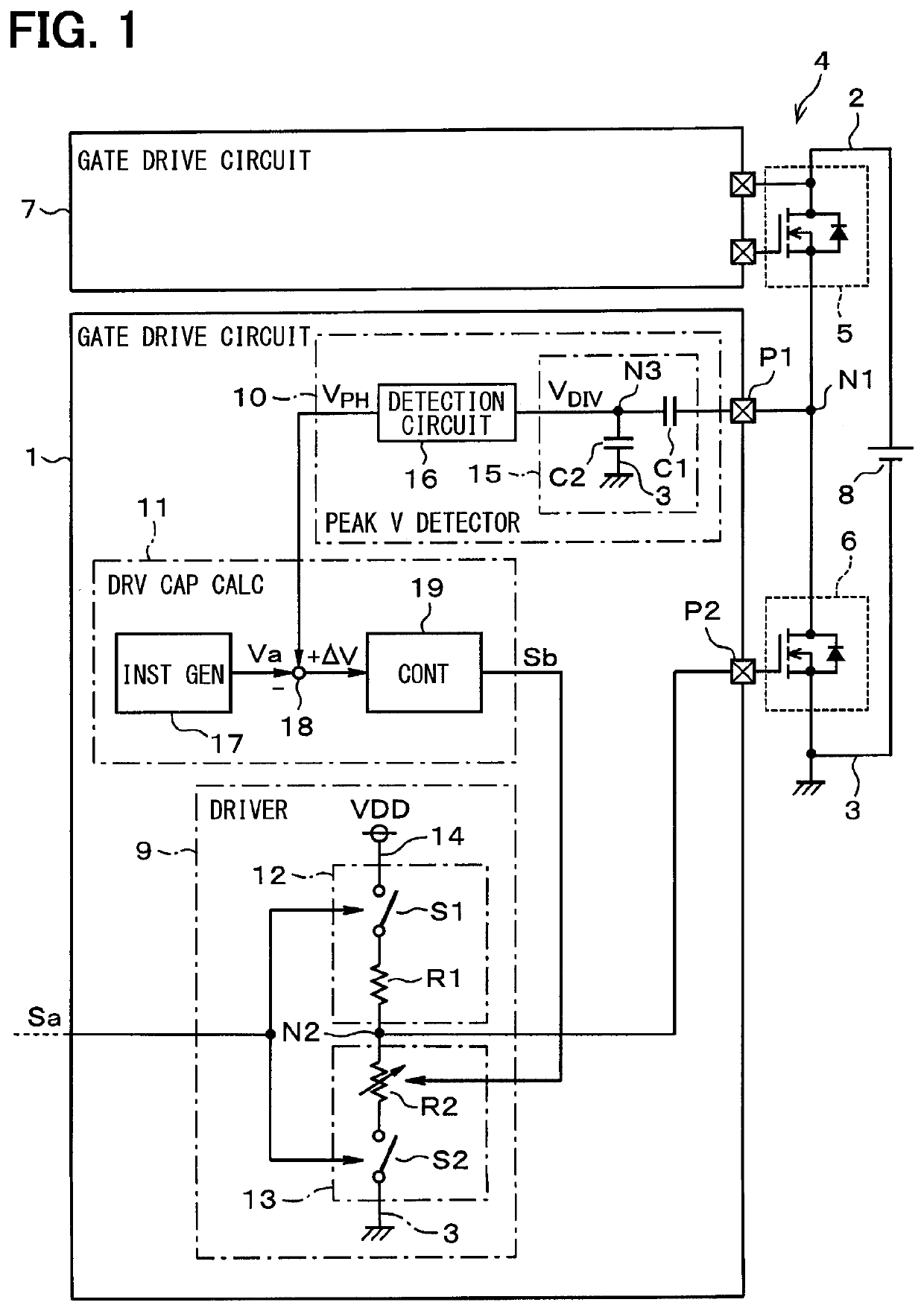
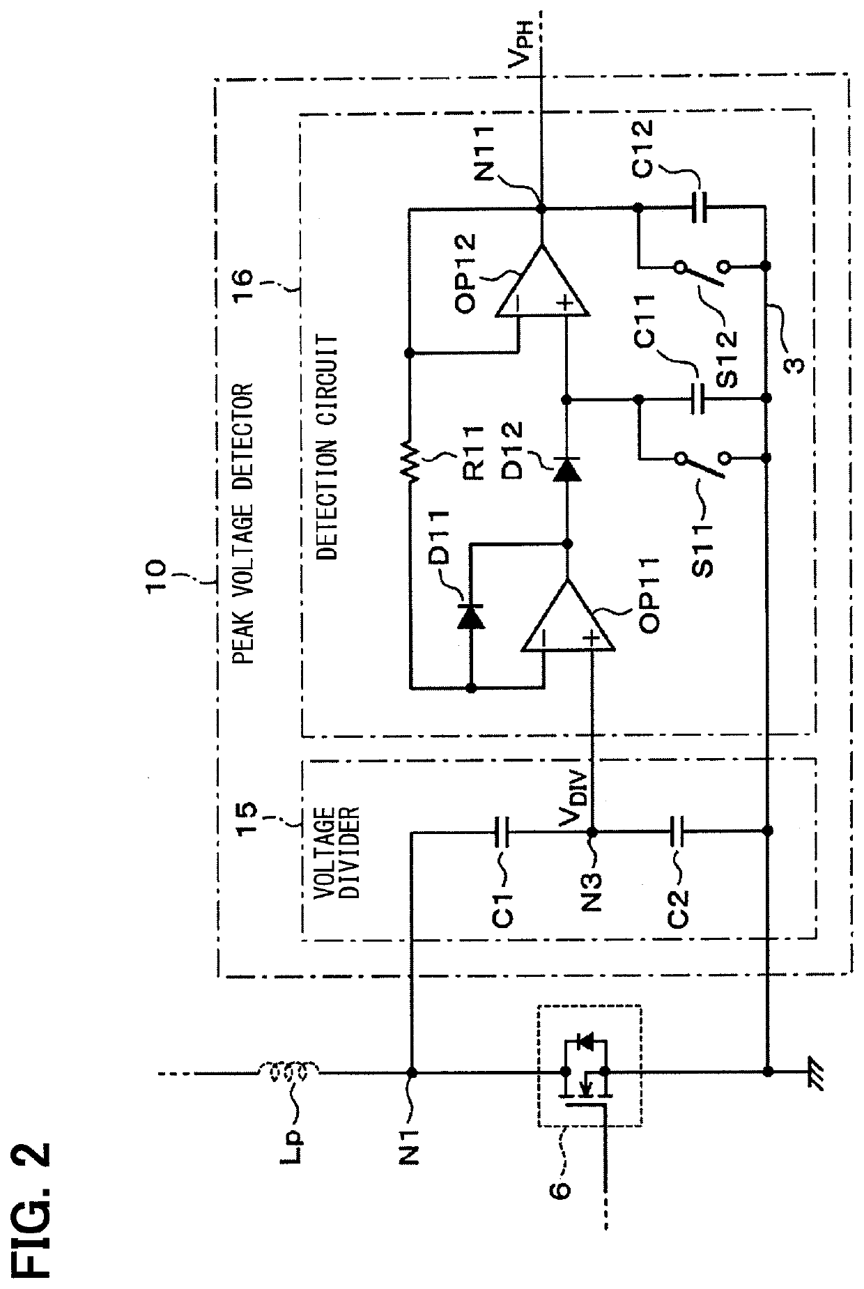
[0027]With reference to FIG. 1, a gate drive circuit 1 of the present embodiment is used to drive a gate of a switching element 6. The switching element 6 is one of a pair of switching elements along with a switching element 5 that together form a half-bridge circuit 4. The switching element 6 is on a low potential side of the half-bridge circuit 4, and the switching element 5 is on a high potential side of the half-bridge circuit 4. The switching elements 5 and 6 are respectively connected at a position between a pair of direct current (DC) power supply lines 2 and 3. The switching element 5 on the high potential side is driven by a gate drive circuit 7. The drive of the switching elements 5 and 6 is PWM controlled based on externally provided control signals.

[0028]The switching elements 5 and 6 are power elements such as transistors. For example, in the present embodiment, the switching e...

second embodiment

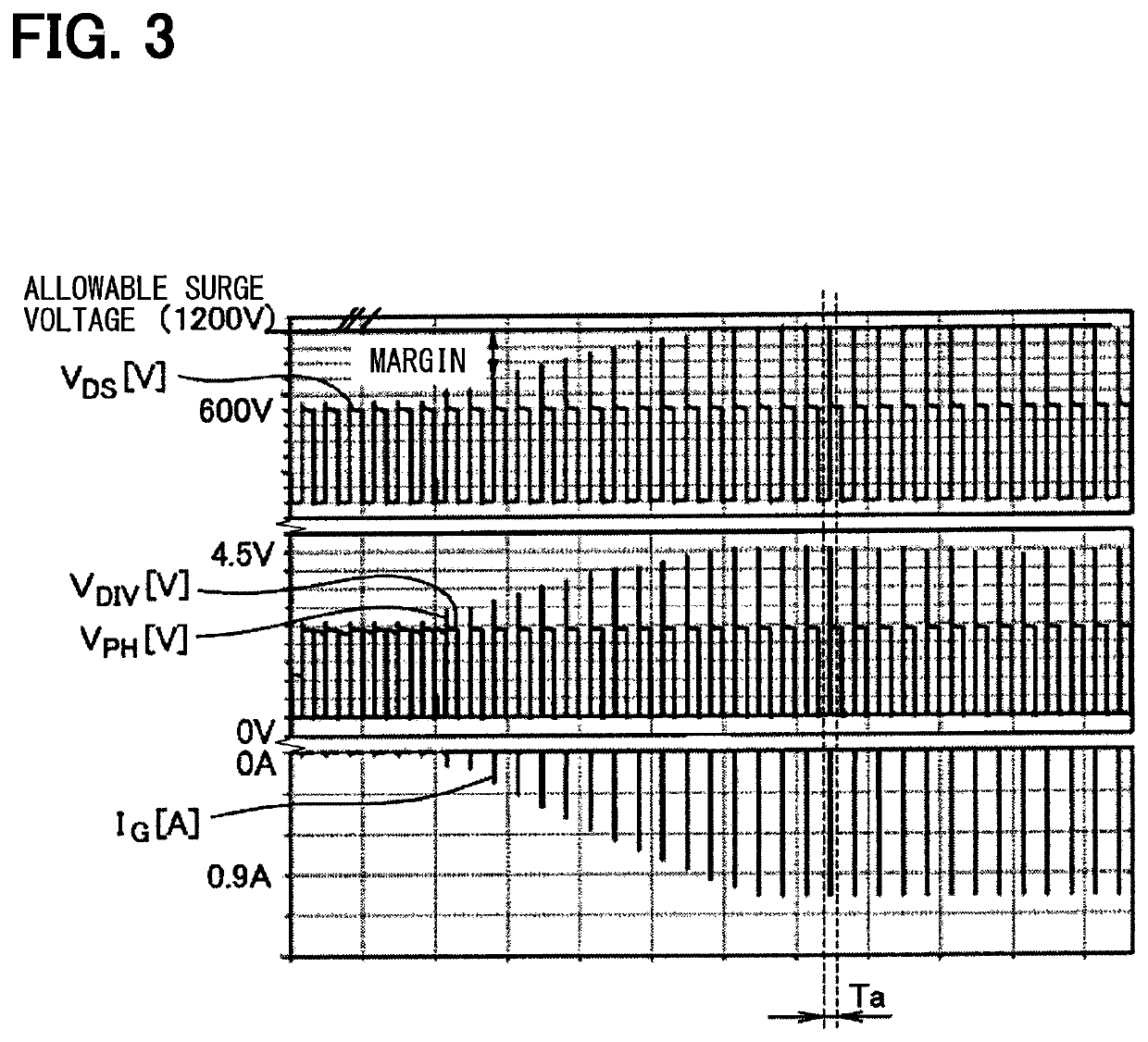
[0075]The second embodiment of the present disclosure is described with reference to FIGS. 5 and 6. When the switching element is driven with a predetermined drive capacity, if the load current changes, the surge voltage also changes based on the change of the load current. More specifically, if the drive capacity, that is, the resistance value of the gate resistor R2, is constant, the peak of the surge voltage rises as the load current increases, and the peak of the surge voltage decreases as the load current decreases.

[0076]When the surge voltage rises in instances where the drive capacity is optimized, a voltage exceeding a breakdown voltage of the switching element 24 may be applied to the main terminal of the switching element 24. For example, as shown in FIG. 5, when the load current is 50 A and the load current changes to 75 A in a state where the drive capacity is optimized, the peak surge voltage can exceed the breakdown voltage of the switching element 24.

[0077]When the su...

third embodiment

[0090]The third embodiment of the present disclosure is described with reference to FIGS. 7 and 8. When the switching element 6 is driven with a predetermined drive capacity, if the power supply voltage changes, the surge voltage also changes based on the change of the power supply voltage. More specifically, if the drive capacity (i.e., the resistance value of the gate resistor R2) is constant, the peak of the surge voltage increases as the power supply voltage increases, and the peak of the surge voltage decreases as the power supply voltage decreases. The power supply voltage is a voltage of the DC power supply 8, and corresponds to the drain-source voltage VDS of the switching element 6 during the period when the switching element 6 is turned OFF. In the present embodiment, the power supply voltage may also be referred to as an OFF voltage.

[0091]When the surge voltage rises in instances where the drive capacity is optimized, a voltage exceeding a breakdown voltage may be applied...


PUM


Abstract

A gate drive circuit includes a driver for driving a gate of a switching element, a peak voltage detector, and a drive capacity calculator. The peak voltage detector detects a peak voltage at a main terminal of the switching element when the switching element is OFF. The drive capacity calculator calculates a voltage difference value between the detected peak voltage and an allowable voltage value at the main terminal of the switching element, where the allowable voltage is based on the specifications of the switching element. The drive capacity calculator changes a drive capacity of the driver to gradually decrease the difference between the detected peak voltage and the allowable voltage.

Description

CROSS REFERENCE TO RELATED APPLICATION[0001]The present application is based on and claims the benefit of priority of Japanese Patent Application No. 2018-132344, filed on Jul. 12, 2018, the disclosure of which is incorporated herein by reference.TECHNICAL FIELD[0002]The present disclosure relates to a gate drive circuit for driving a gate of a switching element.BACKGROUND INFORMATION[0003]In gate drive circuits that drive the gates of switching elements such as insulated-gate bipolar transistors (IGBTs) or metal-oxide-semiconductor field-effect transistors (MOSFETs), surge voltages exceeding the breakdown voltage of the switching element may cause failures in the switching element. The suppression effects by gate drive circuits to mitigate excessive surge voltages may create additional issues in the switching elements. As such, gate drive circuits are subject to improvement.SUMMARY[0004]The present disclosure describes a gate drive circuit for driving a switching element that can s...

Claims


Application Information

Patent Timeline
Patent Type & Authority Applications(United States)
IPC IPC(8): H03K17/00H03K17/16H03K17/082
CPCH03K17/002H03K17/0826H03K17/0822H03K17/168H03K17/0828H03K17/567H03K17/687H03K2217/0036H03K2217/0081H03K2217/0054Y02B70/10
Inventor YAMAMOTONIWA, AKIMASA
Owner DENSO CORP
Why Eureka
Try Eureka