
Photodissociation Frame Window, Systems Including a Photodissociation Frame Window, and Methods of Using a Photodissociation Frame Window

a technology photodissociation frame window, which is applied in the field of photodissociation frame window system, can solve problems such as damage in the latter imprinting step

Active Publication Date: 2020-01-23
CANON KK
View PDF0 Cites 8 Cited by
  • Summary
  • Abstract
  • Description
  • Claims
  • Application Information

AI Technical Summary

Benefits of technology

The patent offers a way to remove material from a template without damaging the pattern area coating. This is achieved by preventing the reactive gas from reaching the pattern area while removing material from the sides.

Problems solved by technology

These extrusions can cause damage in latter imprinting steps.

Method used


Image

  • Photodissociation Frame Window, Systems Including a Photodissociation Frame Window, and Methods of Using a Photodissociation Frame Window
  • Photodissociation Frame Window, Systems Including a Photodissociation Frame Window, and Methods of Using a Photodissociation Frame Window
  • Photodissociation Frame Window, Systems Including a Photodissociation Frame Window, and Methods of Using a Photodissociation Frame Window

Examples


Embodiment Construction

[0040]What is needed is a system and / or method that prevents extrusions from forming on the sidewalls or removing extrusions from sidewalls while protecting the pretreated patterning surface.

Nanoimprint System

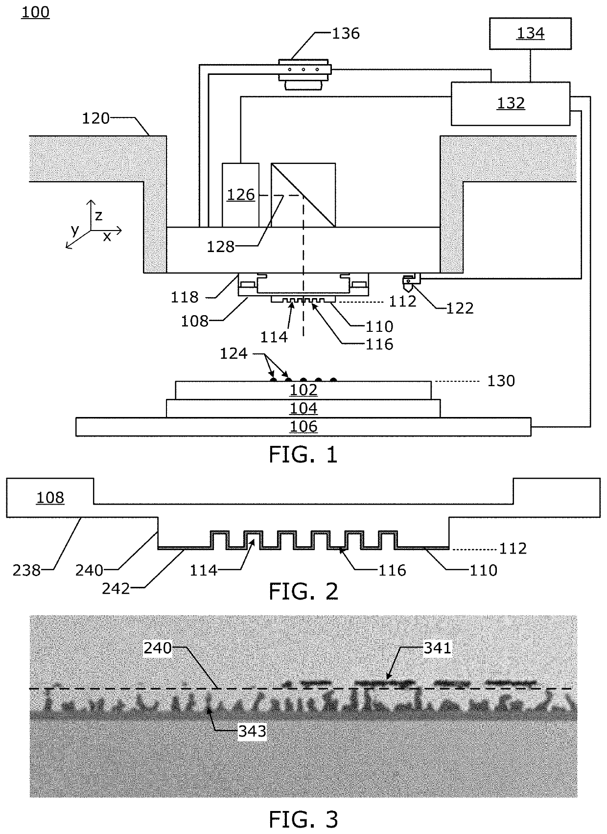
[0041]FIG. 1 is an illustration of a nanoimprint lithography system 100 in which an embodiment may be implemented. The nanoimprint lithography system 100 is used to form a relief pattern on a substrate 102. The substrate 102 may be coupled to a substrate chuck 104. The substrate chuck 104 may be but is not limited to a vacuum chuck, pin-type chuck, groove-type chuck, electrostatic chuck, electromagnetic chuck, and / or the like.

[0042]The substrate 102 and the substrate chuck 104 may be further supported by a substrate positioning stage 106. The substrate positioning stage 106 may provide translational and / or rotational motion along one or more of the x, y, z, θ, and φ-axes. The substrate positioning stage 106, the substrate 102, and the substrate chuck 104 may also be positioned ...


PUM

PropertyMeasurementUnit
Fractionaaaaaaaaaa
Wavelengthaaaaaaaaaa
Electrical resistanceaaaaaaaaaa

Abstract

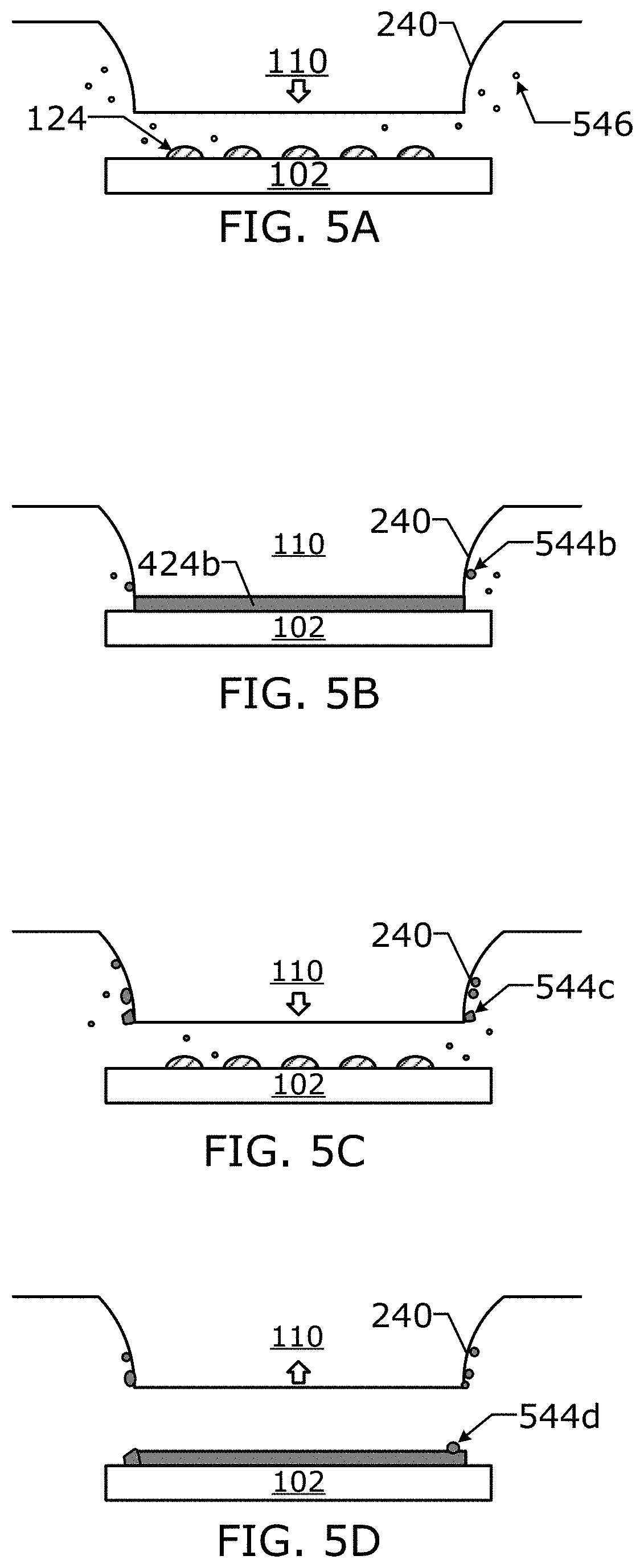
An apparatus, method, and frame window configured to clean mesa sidewalls of a template with photodissociation radiation. Material on the mesa sidewalls are removed from the mesa sidewalls by exposing the portion of a first gap adjacent to the mesa sidewalls to the photodissociation radiation.

Description

BACKGROUNDField of Art[0001]The present disclosure relates to a photodissociation frame window systems and methods of using photodissociation frame window for cleaning mesa sidewalls of a template while protecting a patterning surface of the template from modification.Description of the Related Art[0002]Nano-fabrication includes the fabrication of very small structures that have features on the order of 100 nanometers or smaller. One application in which nano-fabrication has had a sizeable impact is in the fabrication of integrated circuits. The semiconductor processing industry continues to strive for larger production yields while increasing the circuits per unit area formed on a substrate. Improvements in nano-fabrication include providing greater process control and / or improving throughput while also allowing continued reduction of the minimum feature dimensions of the structures formed.[0003]One nano-fabrication technique in use today is commonly referred to as nanoimprint lith...

Claims


Application Information

Patent Timeline
IPC IPC(8): G03F7/00B29C59/02B29C35/08
CPCB29C59/022B82Y40/00G03F7/0002B29C2035/0833B29C2035/0827B29C35/0805
Inventor FLETCHER, EDWARD BRIAN
Owner CANON KK
Learn More