Electrochemical doping of thin metal layers employing underpotential deposition and thermal treatment

a thin metal layer and underpotential deposition technology, applied in the direction of liquid/solution decomposition chemical coating, semiconductor/solid-state device details, coatings, etc., can solve the problem of scaling the barrier layer beyond certain critical dimensions, and achieve the effect of superior adhesion and barrier properties

Active Publication Date: 2020-02-27
LAM RES CORP
View PDF0 Cites 2 Cited by
  • Summary
  • Abstract
  • Description
  • Claims
  • Application Information

AI Technical Summary

Benefits of technology

The present disclosure provides a method for doping liner materials with a electronegative element to improve adhesion and barrier properties for future technology nodes. The doping can be achieved through underpotential deposition and a heat treatment process, which causes migration of the element to an interface of the liner and an oxide layer of the substrate or a dielectric layer. The technique helps to create a barrier-less metallization scheme, which has superior adhesion and barrier properties.

Problems solved by technology

However, with the continuous shrinkage in the size of the technology nodes, it is challenging to scale the barrier layer beyond certain critical dimensions.

Method used


Image

  • Electrochemical doping of thin metal layers employing underpotential deposition and thermal treatment
  • Electrochemical doping of thin metal layers employing underpotential deposition and thermal treatment
  • Electrochemical doping of thin metal layers employing underpotential deposition and thermal treatment

Examples


Embodiment Construction

[0031]In the following description, numerous specific details are set forth to provide a thorough understanding of the presented embodiments. The disclosed embodiments may be practiced without some or all of these specific details. In other instances, well-known process operations have not been described in detail to not unnecessarily obscure the disclosed embodiments. While the disclosed embodiments will be described in conjunction with the specific embodiments, it will be understood that it is not intended to limit the disclosed embodiments.

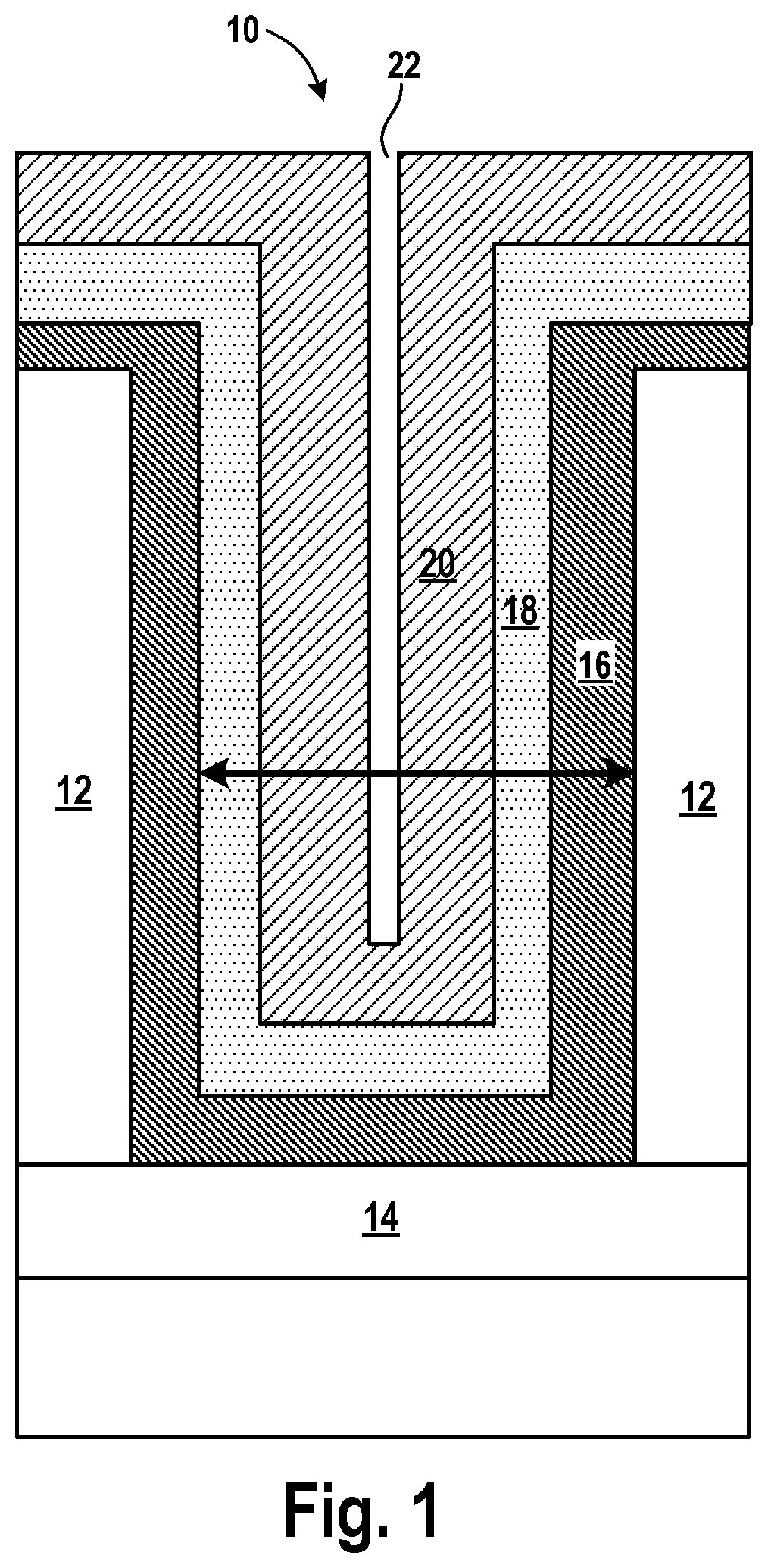
[0032]In keeping with Moore's Law, there has been a continual drive towards smaller and smaller feature sizes in the semiconductor industry. At present, semiconductor manufacturers are commonly producing devices with a 28 nanometer (nm) feature size, or approximately 28 nm pitch. Devices with a 36 nm pitch size are expected to soon. Typically, the pitch is halved every two technology nodes. Thus, it is expected that within about two to three no...


PUM

PropertyMeasurementUnit
sizeaaaaaaaaaa
sizeaaaaaaaaaa
pitch sizeaaaaaaaaaa

Abstract

A method is provided, including the following operations: depositing a liner in a feature of a substrate; depositing a monolayer of zinc over the liner; after depositing the monolayer of zinc, performing a thermal treatment on the substrate, wherein the thermal treatment is configured to cause migration of the zinc to an interface of the liner and an oxide layer of the substrate, the migration of the zinc producing an adhesive barrier at the interface that improves adhesion between the liner and the oxide layer of the substrate; repeating the operations of depositing the monolayer of zinc and performing the thermal treatment until a predefined number of cycles is reached.

Description

FIELD OF THE INVENTION[0001]Implementations of the present disclosure relate to electrochemical doping of thin metal layers employing underpotential deposition and thermal treatment, and related methods, apparatus, and systems.DESCRIPTION OF THE RELATED ART[0002]Copper (Cu) is used as an interconnect material for the fabrication of advanced semiconductor devices. Under a current process, the Cu metallization scheme entails deposition of a Cu / Ru / TaN (or Cu / Co / TaN) stack in the interconnect structure, e.g. over an underlying conductor and SiO2. TaN serves a barrier layer to prevent the Cu from diffusing into the SiO2 layer and Ru (or Co) acts as a liner to enable Cu deposition providing lower electrical resistance than TaN. However, with the continuous shrinkage in the size of the technology nodes, it is challenging to scale the barrier layer beyond certain critical dimensions.SUMMARY[0003]Implementations of the present disclosure provide an electrochemical technique of doping liner m...

Claims


Application Information

Patent Timeline
Patent Type & Authority Applications(United States)
IPC IPC(8): C23C16/40H01L21/02C23C16/04C23C18/16H01L21/768C23C18/54C23C16/06
CPCC23C16/06C23C16/045H01L21/76871C23C18/38C23C18/1653C23C18/54C23C18/1692H01L21/02266C23C16/408C23C16/406H01L21/02271C23C16/407H01L21/76838H01L21/76843H01L21/76831H01L21/76858H01L21/76855H01L21/76847H01L21/76877H01L21/2885H01L23/53209H01L23/53252H01L23/53238C23C18/1651C25D5/18C25D5/50C25D5/10H01L21/76895
Inventor VENKATRAMAN, KAILASHDORDI, YEZDIJOI, ANIRUDDHA
Owner LAM RES CORP
Why Eureka
Try Eureka