Chip resistor and method for manufacturing same
a technology of chip resistors and manufacturing methods, applied in the direction of resistor chip manufacture, resistor mounting/supporting, resistors adapted for applying terminals, etc., can solve the problems of weakening the protection of the top electrode, the edge of the protective layer is vulnerable to sulfuric gas ingress, and the electrical continuity of the electrodes of the chip resistors is broken. , to achieve the effect of improving the resistance to sulfurization
- Summary
- Abstract
- Description
- Claims
- Application Information
AI Technical Summary
Benefits of technology
Problems solved by technology
Method used
Image

Examples
first embodiment
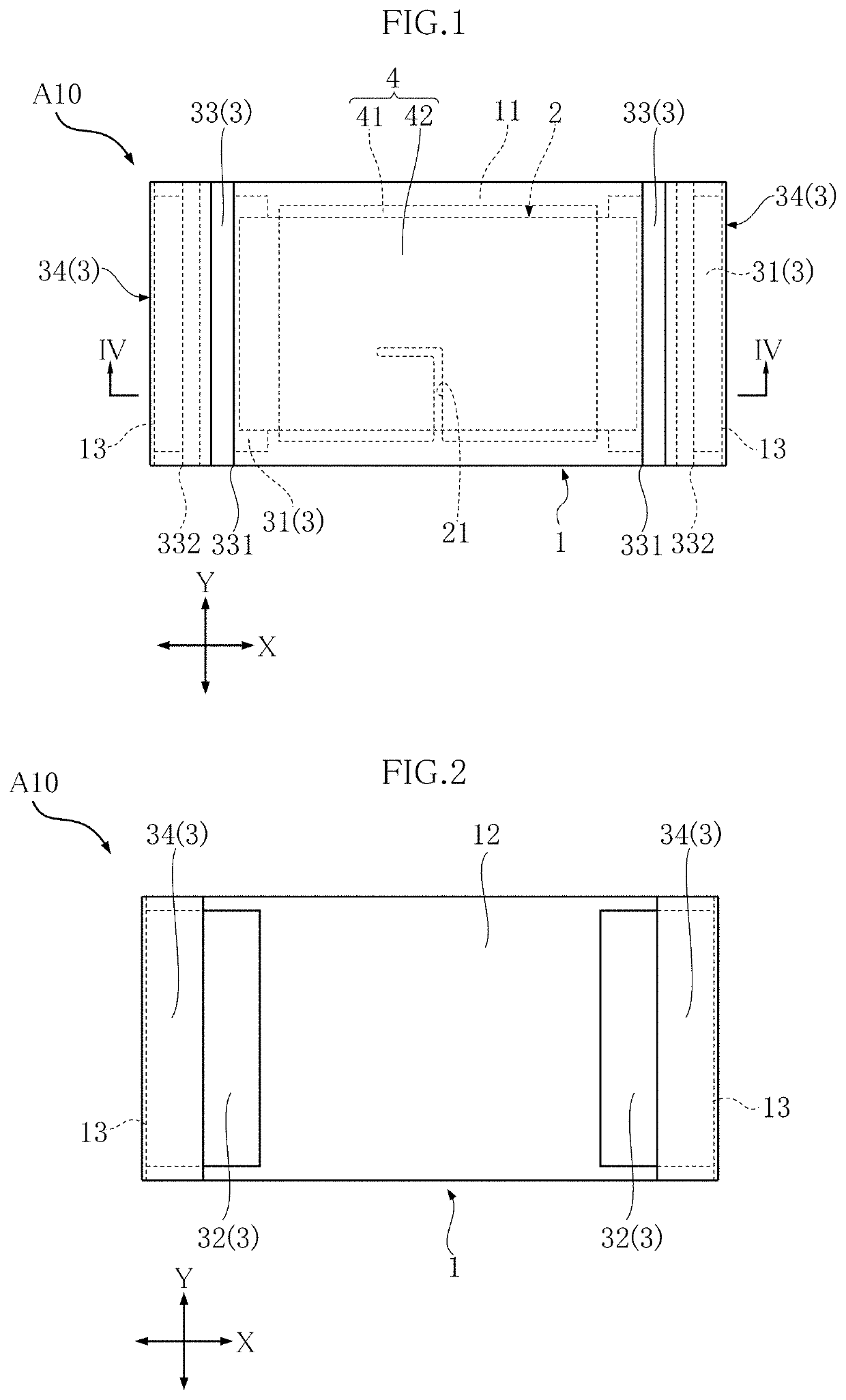
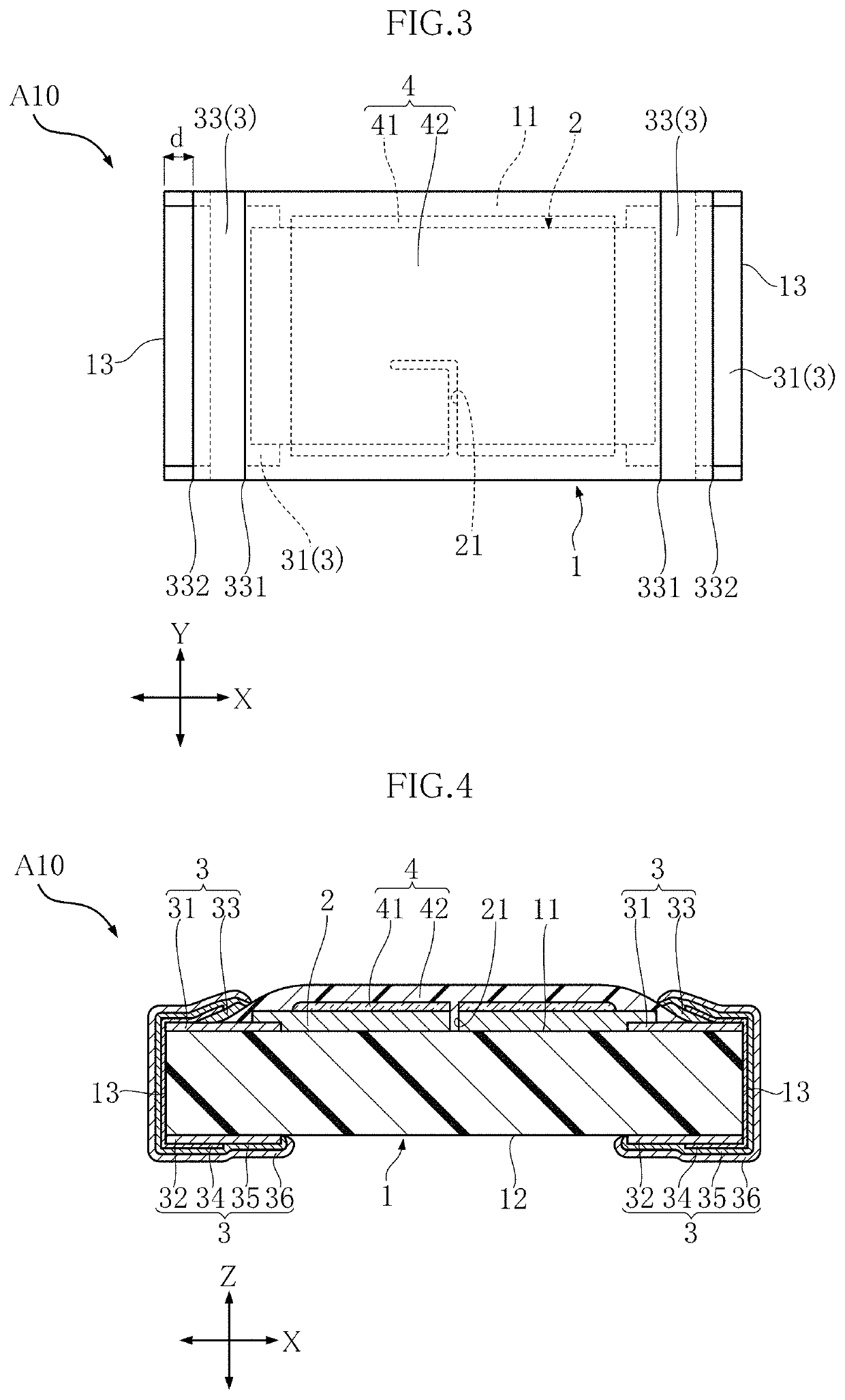
[0035]With reference to FIGS. 1 to 6, the following describes a chip resistor A10 according to a first embodiment of the present disclosure. The chip resistor A10 includes a substrate 1, a resistor 2, electrodes 3 and a protective layer 4.
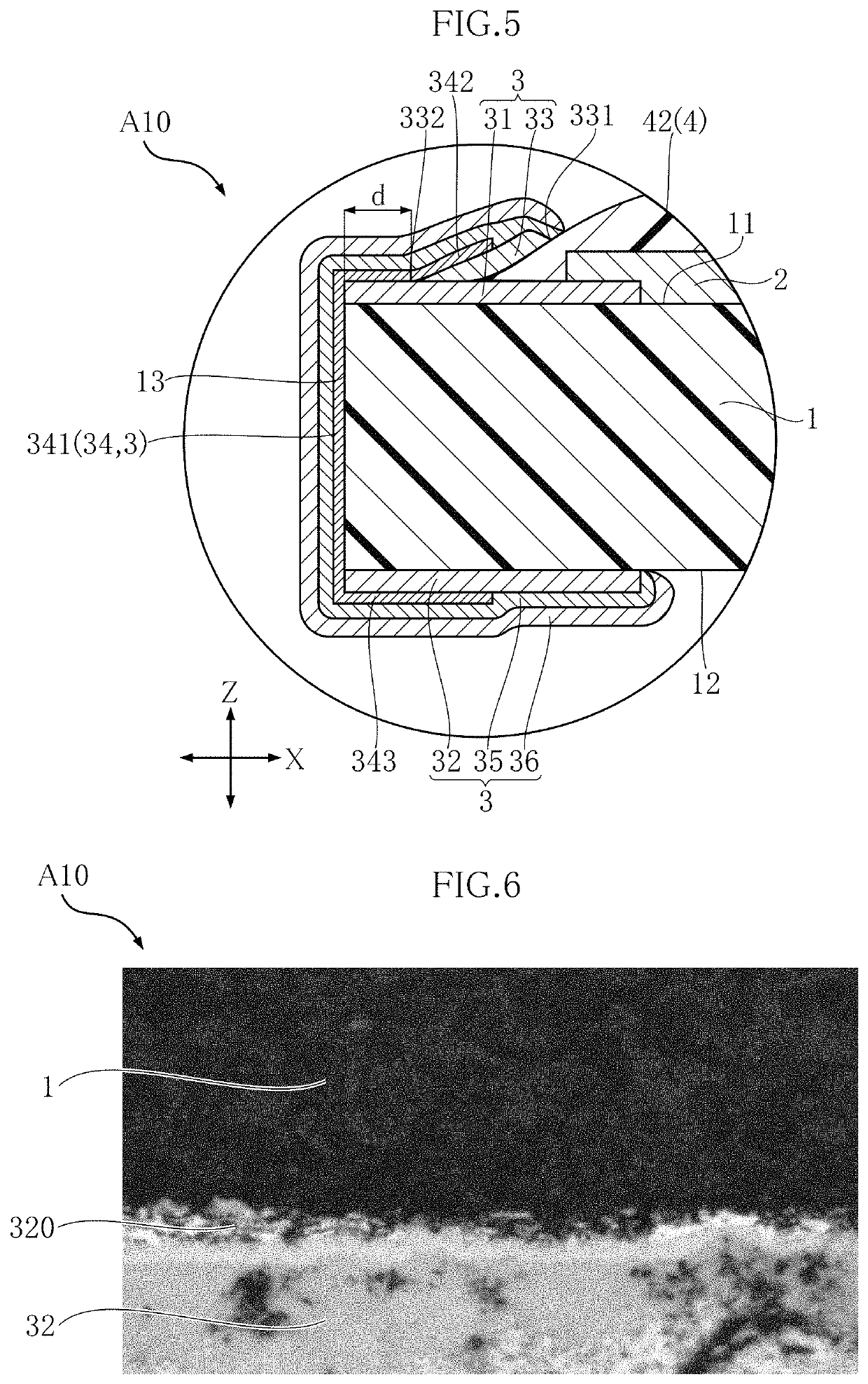
[0036]FIG. 1 is a plan view of the chip resistor A10, and FIG. 2 is a bottom view of the chip resistor A10. For convenience, FIGS. 1 and 2 are seen through intermediate electrodes 35 and outer electrodes 36, which are parts of the electrodes 3 as will be described later. FIG. 3 is a plan view corresponding to FIG. 1 seen through side electrodes 34, which are parts of the electrodes 3 as will be described later. FIG. 4 is a sectional view taken along line IV-IV of FIG. 1. FIG. 5 is a partially enlarged view of FIG. 4. FIG. 6 is a partially enlarged sectional view of a back electrode 32, which is a part of the electrodes 3 of the chip resistor A10 as will be described later.
[0037]The chip resistor A10 shown in the figures is suited for surface mounti...
second embodiment
[0074]With reference to FIGS. 20 and 21, the following describes a chip resistor A20 according to a second embodiment of the present disclosure. In these figures, the same or similar components to those of the chip resistor A10 are denoted by the same reference signs and not described to avoid redundancy.
[0075]FIG. 20 is a sectional view of the chip resistor A20. The position and range of the section shown in FIG. 20 correspond to the section of the chip resistor A10 shown in FIG. 4. FIG. 21 is a partially enlarged view of FIG. 20. In plan view, the chip resistor A20 has the same shape and size as the chip resistor A10.
[0076]The chip resistor A20 differs from the chip resistor A10 in the configuration of the back electrodes 32.
[0077]As shown in FIGS. 20 and 21, each back electrode 32 of the present embodiment includes a first layer 321 and a second layer 322. The first layer 321 is in contact with the back surface 12 of the substrate 1 and made of a synthetic resin, which is an elec...
third embodiment
[0080]With reference to FIGS. 22 to 25, the following describes a chip resistor A30 according to a third embodiment of the present disclosure. In these figures, the same or similar components to those of the chip resistor A10 are denoted by the same reference signs and not described to avoid redundancy.
[0081]FIG. 22 is a plan view of the chip resistor A30 seen through the intermediate electrodes 35 and the outer electrodes 36 of the electrodes 3 for convenience. FIG. 23 is a plan view corresponding to FIG. 22, seen further through the side electrodes 34 of the electrodes 3 for convenience. FIG. 24 is a sectional view taken along line XXIV-XXIV of FIG. 22. FIG. 25 is a partially enlarged view of FIG. 24.
[0082]The chip resistor A30 differs from the chip resistor A10 in the configuration of the protective electrodes 33 and the upper protective layer 42.
[0083]As shown in FIGS. 22 to 25, each protective electrode 33 is sandwiched between a top electrode 31 and a side electrode 34 in the ...
PUM
 Abstract
Description
Claims
Application Information
 - R&D
- Intellectual Property
- Life Sciences
- Materials
- Tech Scout
- Unparalleled Data Quality
- Higher Quality Content
- 60% Fewer Hallucinations
Browse by: Latest US Patents, China's latest patents, Technical Efficacy Thesaurus, Application Domain, Technology Topic, Popular Technical Reports.
© 2025 PatSnap. All rights reserved.Legal|Privacy policy|Modern Slavery Act Transparency Statement|Sitemap|About US| Contact US: help@patsnap.com