
Semiconductor device

a technology of semiconductor chips and insulating films, which is applied in the direction of semiconductor devices, semiconductor/solid-state device details, electrical equipment, etc., can solve the problems of wire peeling and cracking of wires disposed under low-k insulating films, and achieve the effect of preventing peeling and cracking of semiconductor chips, and enhancing reliability

Active Publication Date: 2020-03-05
SAMSUNG ELECTRONICS CO LTD
View PDF0 Cites 0 Cited by
  • Summary
  • Abstract
  • Description
  • Claims
  • Application Information

AI Technical Summary

Benefits of technology

The patent provides a way to make a semiconductor device that is more reliable. This is done by forming an insulating film with a cutting edge along a scribe line on the device. This prevents peeling and cracking defects that can occur when the device is cut.

Problems solved by technology

Meanwhile, when a low-k insulating film is used in the semiconductor device, a peeling phenomenon of wires disposed under the low-k insulating film may occur.

Method used


Image

  • Semiconductor device
  • Semiconductor device
  • Semiconductor device

Examples


Embodiment Construction

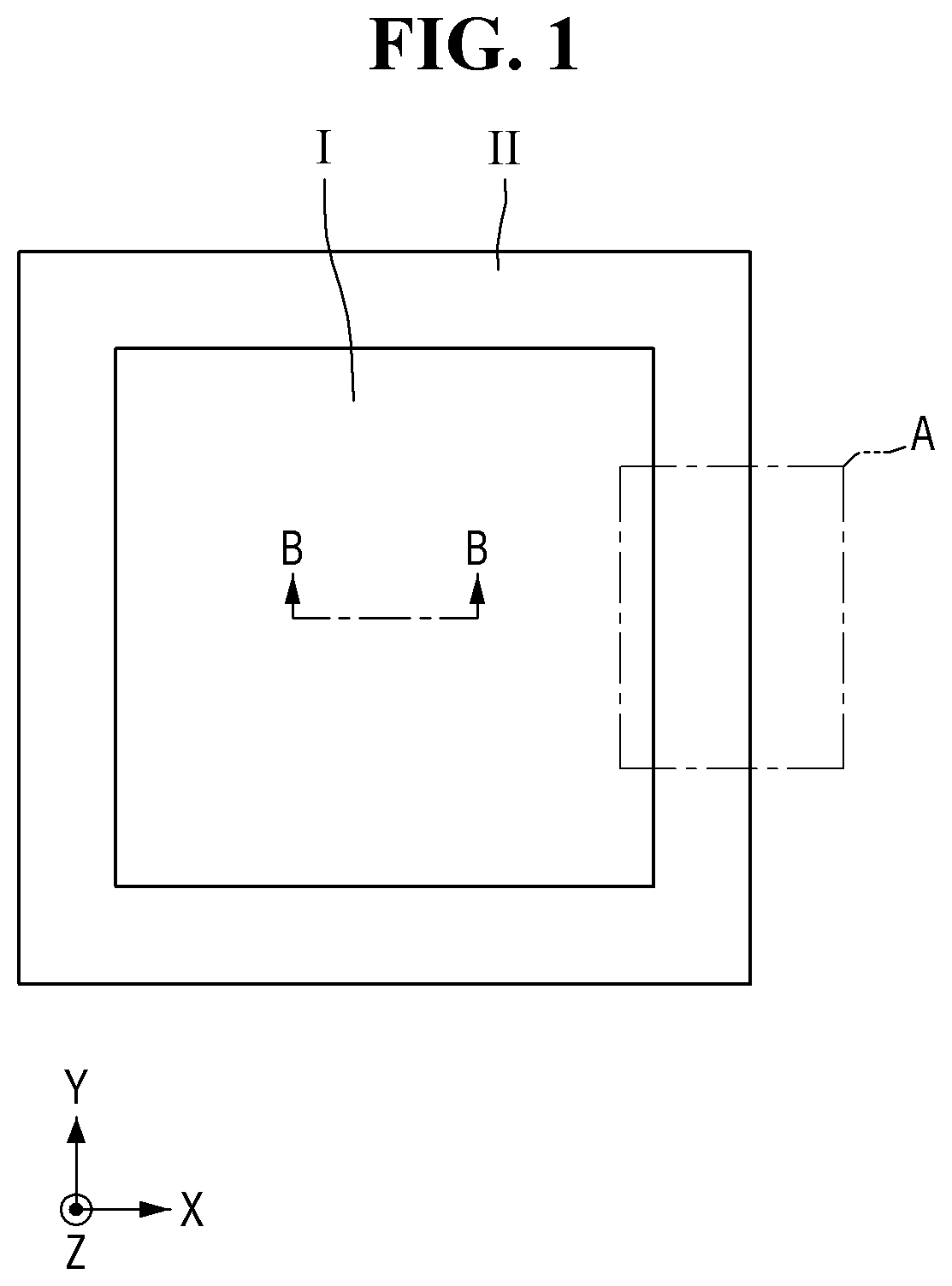
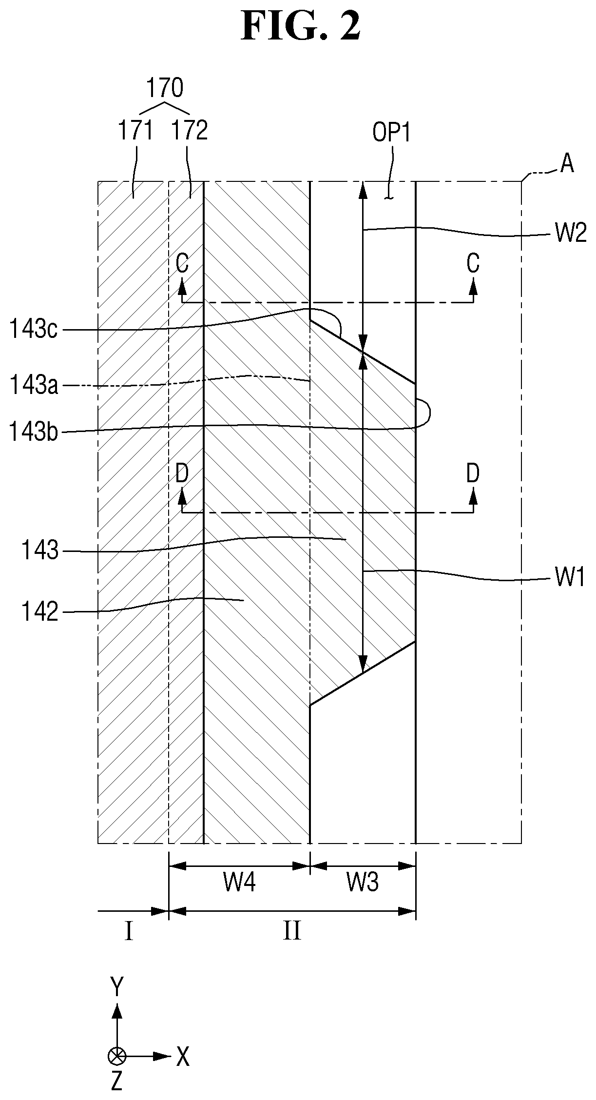
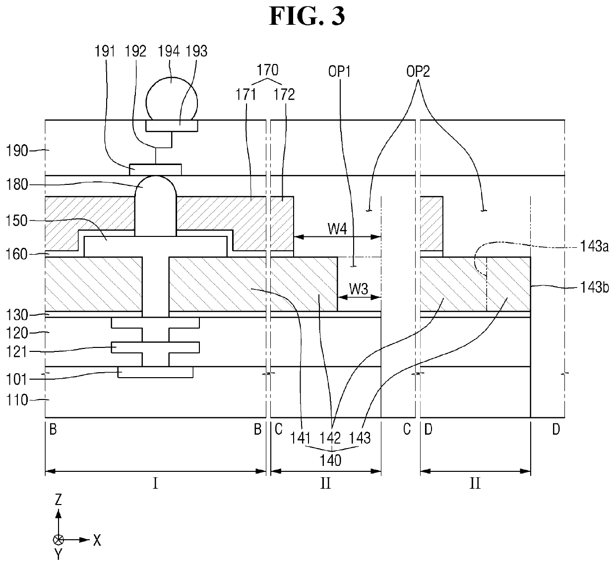
[0023]Hereinbelow, a semiconductor device according to some exemplary embodiments will be described with reference to FIG. 1 to FIG. 3. In the present disclosure, the phrase “at least one of A and B” includes “only A”, “only B”, and “both A and B”.

[0024]FIG. 1 is a top view provided to explain a semiconductor device according to some exemplary embodiments; FIG. 2 is an enlargement view of a region A in FIG. 1; FIG. 3 is a cross-sectional view taken on lines B-B of FIG. 1, C-C and D-D of FIG. 2; FIG. 1 and FIG. 2 do not illustrate a base substrate 190 for convenience of explanation.

[0025]Referring to FIG. 1 to FIG. 3, the semiconductor device according to some exemplary embodiments may include a substrate 110, a first insulating film 120, an etch stop film 130, a second insulating film 140, a rewire layer 150, a passivation film 160, a photo sensitive film 170, a connection terminal 180 and a base substrate 190.

[0026]The substrate 110 may be a structure in which the base substrate an...


PUM

PropertyMeasurementUnit
dielectric constantaaaaaaaaaa
widthaaaaaaaaaa
distanceaaaaaaaaaa

Abstract

A semiconductor device is provided. The semiconductor device includes a substrate, an insulating film, and a photo sensitive film. The substrate includes a semiconductor chip region and a scribe line region disposed along an edge of the semiconductor chip region. The insulating film includes a first portion disposed on the semiconductor chip region, a second portion disposed on the scribe line region and connected with the first portion, and a third portion disposed on the scribe line region and protruded in a first direction from the second portion. The photo sensitive film is disposed on the insulating film and has a sidewall exposed on the second portion of the insulating film. A first width of the third portion in a second direction perpendicular to the first direction decreases as a distance from the semiconductor chip region increases.

Description

[0001]This application claims priority to Korean Patent Application No. 10-2018-0102533, filed on Aug. 30, 2018 in the Korean Intellectual Property Office, and all the benefits accruing therefrom under 35 U.S.C. § 119, the disclosure of which is incorporated by reference herein in its entirety.BACKGROUND1. Technical Field[0002]The present disclosure relates to a semiconductor device.2. Description of the Related Art[0003]Recently, a semiconductor device is advancing in miniaturization and high performance. Accordingly, a low-k insulating film may be used in the semiconductor device.[0004]When the semiconductor device is cut off for packaging of the semiconductor device, physical stress may be applied to the semiconductor device. Meanwhile, when a low-k insulating film is used in the semiconductor device, a peeling phenomenon of wires disposed under the low-k insulating film may occur.SUMMARY[0005]It is an aspect to provide a semiconductor device having enhanced reliability as an ope...

Claims


Application Information

Patent Timeline
Patent Type & Authority Applications(United States)
IPC IPC(8): H01L23/31H01L21/78H01L23/00
CPCH01L2224/02313H01L24/13H01L23/3192H01L21/78H01L2224/13024H01L24/02H01L2224/0236H01L23/3178H01L23/5283H01L23/5329H01L23/562H01L2224/0239H01L24/05H01L2224/0401H01L2224/05548H01L2224/0391H01L2924/15311H01L2224/16227H01L2224/13022H01L24/16H01L23/3171H01L2224/05647H01L2224/05644H01L2224/05611H01L2224/05618H01L2224/05669H01L2224/05609H01L2224/05664H01L2224/05655H01L2224/05639H01L2224/05671H01L2224/81399H01L2224/05666H01L2224/05693H01L2224/13099H01L2224/05624H01L2224/05616H01L2924/013H01L2924/00014H01L2924/01006H01L23/12H01L21/76H01L23/48H01L2223/5446
Inventor CHO, HO SUNGLEE, SANG KWEONKIM, SANG YOUNG
Owner SAMSUNG ELECTRONICS CO LTD
Features
  • Generate Ideas
  • Intellectual Property
  • Life Sciences
  • Materials
  • Tech Scout
  • Unparalleled Data Quality
  • Higher Quality Content
  • 60% Fewer Hallucinations
Learn More