Method for manufacturing active array switch

a technology of active array switch and manufacturing method, which is applied in the direction of basic electric elements, electrical apparatus, and semiconductor devices, can solve the problems of switching without semiconductor characteristics, affecting the and not being applicable to the current production line of a mainstream product, etc., and achieves the effect of stable electric performance of the active array switch

Inactive Publication Date: 2020-03-05
HKC CORP LTD
View PDF0 Cites 0 Cited by
  • Summary
  • Abstract
  • Description
  • Claims
  • Application Information

AI Technical Summary

Benefits of technology

[0017]Due to the improvement made in this application, during a BCE process of an active array switch, a first photoresist layer on a semiconductor layer above a gate pattern (at a TFT back channel) may be reserved, and then a normal film forming etching process may be performed on a source and a drain, to remove a second photoresist

Problems solved by technology

Although having higher mobility, a Poly-Si active array switch is not applicable to the current production line of a mainstream product as a result of relatively high costs.
However, when processing an active array switch with a BCE structure, one of the problems is that an oxide semiconductor layer may be permanently damaged by source and drain etching solutions, affecting electric performance of the active array switch, and even directly leading to that the a

Method used


Image

  • Method for manufacturing active array switch
  • Method for manufacturing active array switch
  • Method for manufacturing active array switch

Examples


Embodiment Construction

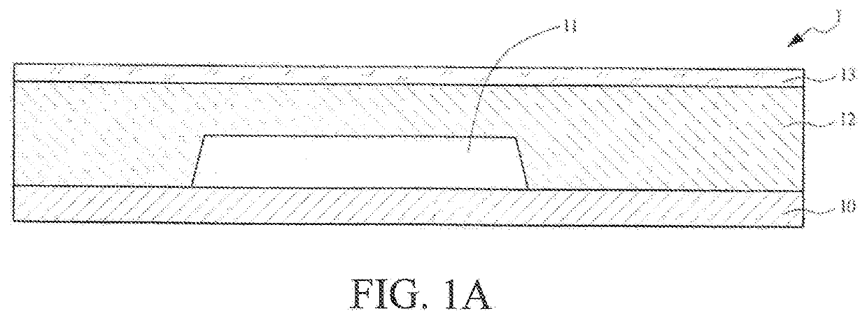
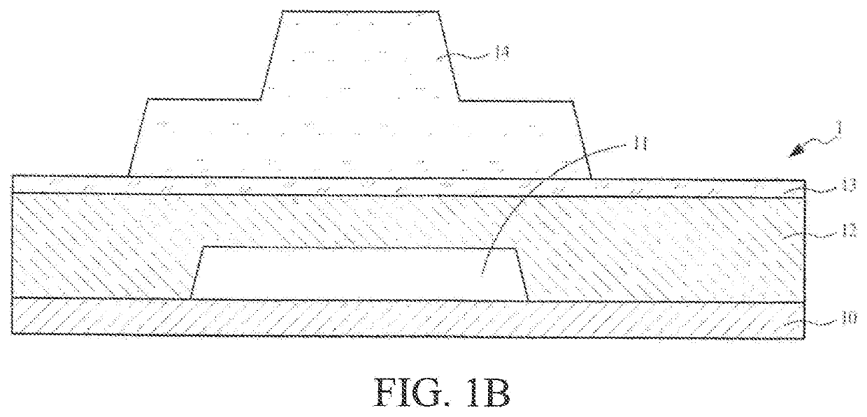
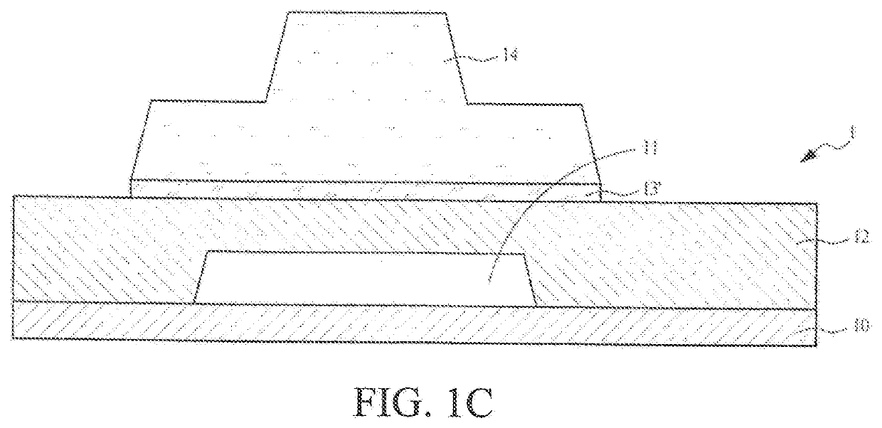
[0027]The following embodiments are described with reference to the accompanying drawings, which are used to exemplify specific embodiments for implementation of this application. Terms about directions mentioned in this application, such as “on”, “below”, “front”, “back”, “left”, “right”, “in”, “out”, and “side surface” merely refer to directions in the accompanying drawings. Therefore, the used terms about directions are used to describe and understand this application, and are not intended to limit this application.

[0028]The accompanying drawings and the description are considered to be essentially exemplary, rather than limitative. In the figures, units with similar structures are represented by using the same reference number. In addition, for understanding and ease of description, the size and the thickness of each component shown in the accompanying drawings are arbitrarily shown, but this application is not limited thereto.

[0029]In the accompanying drawings, for clarity, thi...


PUM


Abstract

This application provides a method for manufacturing an active array switch, including: forming a gate pattern on a substrate, and then forming a gate insulation layer to cover the gate pattern; forming a semiconductor layer on the gate insulation layer, and forming a first photoresist layer having a plurality of thicknesses on the semiconductor layer, where a thickness of the first photoresist layer above the middle part of the gate pattern is greater than a thicknesses of the first photoresist layer above the two sides of the gate pattern; removing the semiconductor layer, to form a semiconductor pattern; performing a dry etching process on the first photoresist layer; forming a source and a drain on the semiconductor pattern and the gate insulation layer, and removing the entire photoresist layer above the source and the drain and the entire photoresist layer above the middle part of the gate pattern.

Description

BACKGROUNDTechnical Field[0001]This application relates to a method for manufacturing an active array switch, and in particular, to a method for manufacturing an active array switch by using which a semiconductor layer can be effectively protected from being affected by source and drain etching solutions.Related Art[0002]Currently, a semiconductor layer in an active array switch driving a display panel mainly includes an amorphous silicon (a-Si) semiconductor layer, an oxide semiconductor layer, a polycrystalline silicon (Poly-Si) semiconductor layer, and the like. Compared with an a-Si semiconductor, an oxide semiconductor has higher mobility and a lower electric leakage rate. Although having higher mobility, a Poly-Si active array switch is not applicable to the current production line of a mainstream product as a result of relatively high costs.[0003]A commonly used structure of an active array switch with an oxide semiconductor includes an etch stop layer (ESL) structure, a back...

Claims


Application Information

Patent Timeline
IPC IPC(8): H01L27/12
CPCH01L27/1222H01L27/1218H01L27/1288H01L29/401H01L29/41733H01L29/42356H01L29/42384H01L29/66969H01L27/1225
Inventor HE, HUAILIANG
Owner HKC CORP LTD
Why Eureka
Try Eureka