Gate-all-around field effect transistors with air-gap inner spacers and methods

a gate-all-around field effect and inner spacer technology, applied in the field of gate-all-around field effect transistors, can solve the problems that the processing techniques of gaafets may no longer be suitable, and no longer allow the proper formation and functioning of inner spacers

Active Publication Date: 2020-03-12
GLOBALFOUNDRIES US INC
View PDF0 Cites 24 Cited by
  • Summary
  • Abstract
  • Description
  • Claims
  • Application Information

AI Technical Summary

Problems solved by technology

However, with continued device size scaling, conventional GAAFET processing techniques may no longer be s

Method used


Image

  • Gate-all-around field effect transistors with air-gap inner spacers and methods
  • Gate-all-around field effect transistors with air-gap inner spacers and methods
  • Gate-all-around field effect transistors with air-gap inner spacers and methods

Examples


Embodiment Construction

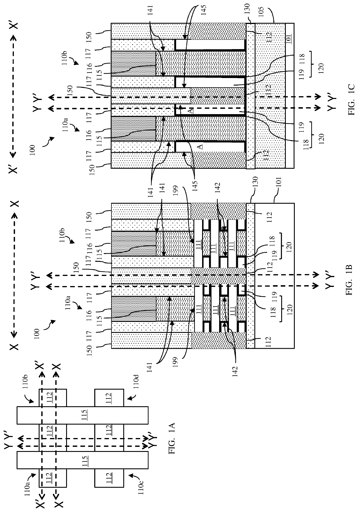
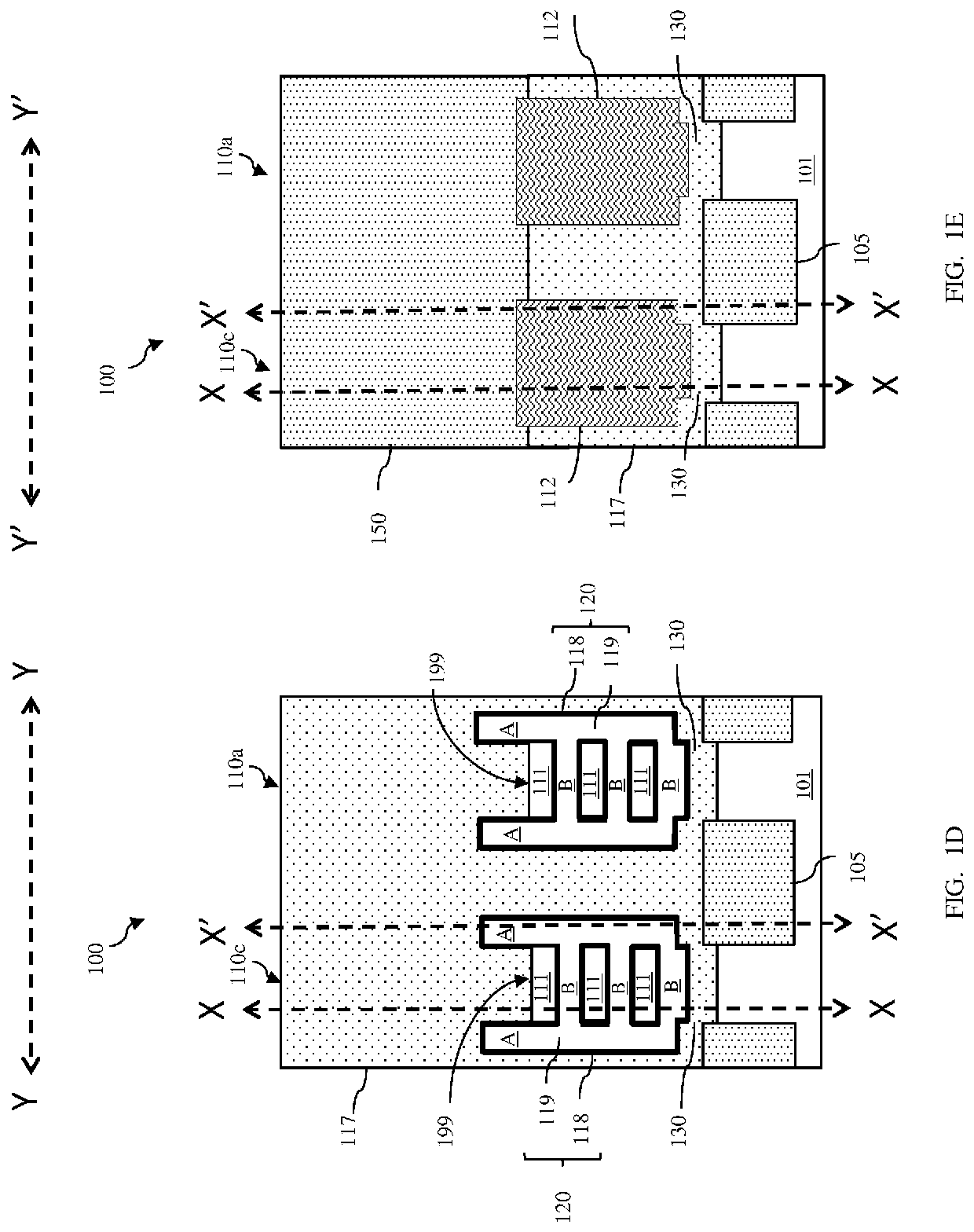
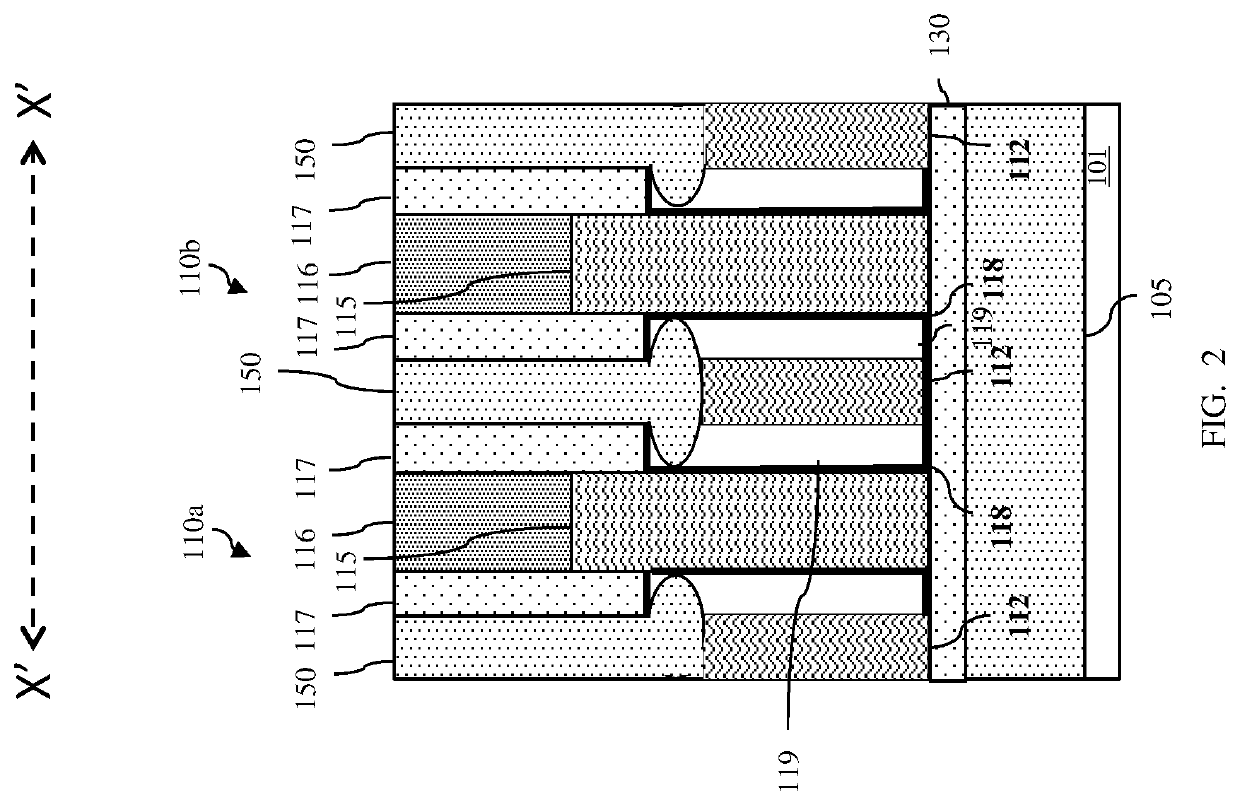
[0036]As mentioned above, to improve device drive current and electrostatics and to allow for further device size scaling, gate-all-around field effect transistors (GAAFETs) (e.g., nanowire-type GAAFETs or nanosheet-type GAAFETs) were developed. A GAAFET includes elongated semiconductor nanoshape(s) (e.g., nanowires or nanosheets), which extend laterally between source / drain regions, and a gate structure, which wraps around (i.e., which is adjacent to the top, bottom and opposing sides) of the center portions of the nanoshape(s) such that the nanoshape(s) function as channel region(s). In such GAAFETs, spacers, including a gate sidewall spacer and inner spacers, provide electrical isolation between the gate and the adjacent source / drain regions. Specifically, a “gate sidewall spacer” refers to a spacer that is positioned laterally adjacent to external sidewalls of the gate structure and “inner spacers” refer to those spacers that are positioned laterally between the source / drain reg...


PUM


Abstract

Disclosed are structures including a gate-all-around field effect transistor (GAAFET) with air-gap inner spacers. The GAAFET includes a stack of nanoshapes that extend laterally between source/drain regions, a gate that wraps around a center portion of each nanoshape, and a gate sidewall spacer on external sidewalls of the gate. The GAAFET also includes air-gap inner spacers between the gate and the source/drain regions. Each air-gap inner spacer includes: two vertical sections within the gate sidewall spacer on opposing sides of the stack and adjacent to a source/drain region; and horizontal sections below the nanoshapes and extending laterally between the vertical sections. Also discloses are methods of forming the structures and the method include forming preliminary inner spacers in inner spacer cavities prior to source/drain region formation. After source/drain regions are formed, the preliminary inner spacers are removed and the cavities are sealed off, thereby forming the air-gap inner spacers.

Description

BACKGROUNDField of the Invention[0001]The present invention relates to gate-all-around field effect transistors (GAAFETs) and, more particularly, to GAAFETs with air-gap inner spacers and methods of forming the GAAFETS.Description of Related Art[0002]Integrated circuit (IC) design decisions are often driven by device performance, scalability, and manufacturability. For example, recently, to improve device drive current and electrostatics and to allow for further device size scaling, gate-all-around field effect transistors (GAAFETs) (e.g., nanowire-type GAAFETs or nanosheet-type GAAFETs) were developed. A GAAFET includes elongated semiconductor nanoshape(s) (e.g., nanowires or nanosheets), which extend laterally between source / drain regions, and a gate structure, which wraps around (i.e., which is adjacent to the top, bottom and opposing sides) of the center portions of the nanoshape(s) such that the nanoshape(s) function as channel region(s). In such GAAFETs spacers, including a ga...

Claims


Application Information

Patent Timeline
IPC IPC(8): H01L29/66H01L29/78H01L29/06H01L29/423
CPCH01L21/31111H01L29/7853H01L29/0673H01L29/6653H01L29/66553H01L29/6681H01L21/3065H01L29/42392H01L29/0653B82Y10/00H01L29/4991H01L29/66439H01L29/66545H01L29/775H01L29/78696
Inventor CHANEMOUGAME, DANIELFROUGIER, JULIENXIE, RUILONG
Owner GLOBALFOUNDRIES US INC
Why Eureka
Try Eureka