

Electrode substrate for transparent light-emitting device display, and manufacturing method therefor
Active Publication Date: 2020-03-19
LG CHEM LTD
View PDF5 Cites 2 Cited by
- Summary
- Abstract
- Description
- Claims
- Application Information
AI Technical Summary
Benefits of technology
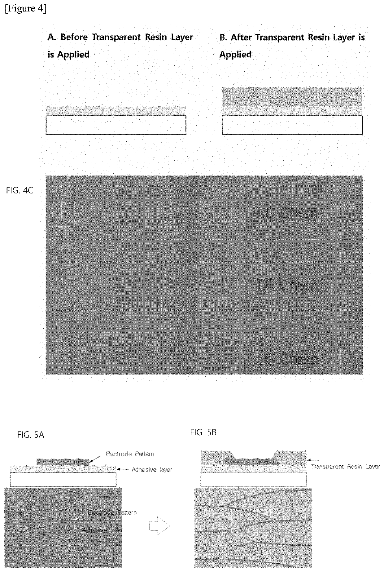
[0011]According to the exemplary embodiment of the present application, a metal pattern is formed by using low-price copper foil, so that it is possible to decrease raw material cost when an electrode substrate for a transparent light emitting device display is manufactured. Particularly, according to the exemplary embodiment of the present application, it is characterized that the transparent photosensitive resin composition layer is formed on the transparent base material and the copper foil pattern, so that it is possible to prevent an increase in haze of the electrode substrate for the transparent light emitting device display due to roughness o
Problems solved by technology
However, reserves of indium, which is a main raw material of the material of the ITO transparent electrode, are not largely available globally and indium is produced in some countries, such as China, and production cost of indium is high.
Further, indium has a disadvantage in that a resistance value is not constantly appli
Method used
View moreImage
Smart ImageViewing Examples

Examples
 PUM
 Abstract
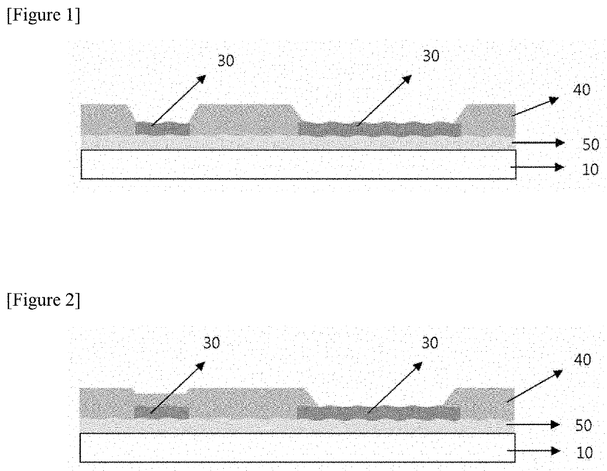
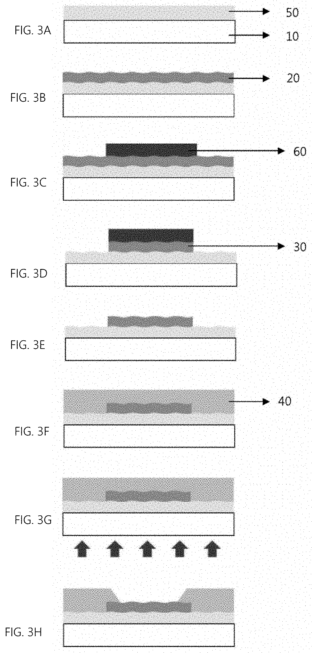
A method of manufacturing an electrode substrate for a transparent light emitting device display that includes laminating copper foil on a transparent base material; forming a copper foil pattern by etching the copper foil; forming a transparent photosensitive resin composition layer on a front surface of the transparent base material and the copper foil pattern; and exposing at least a part of the copper foil pattern by removing at least a part of the transparent photosensitive resin composition layer provided on the copper foil pattern.
Description
TECHNICAL FIELD[0001]This application claims priority to and the benefit of Korean Patent Application No. 10-2017-0120348 filed in the Korean Intellectual Property Office on Sep. 19, 2017, the entire contents of which are incorporated herein by reference.[0002]The present application relates to an electrode substrate for a transparent light emitting device display and a method of manufacturing the same.BACKGROUND ART[0003]Recently, Korea creates various exterior lighting in parks and town centers, as well as colorful signs, and provides information and attraction to urban residents through the convergence of high-tech information and communication technology (ICT) and light emitting diode (LED) technology. Particularly, in a transparent LED display using an indium tin oxide (ITO) transparent electrode material, an LED is applied between glasses or a transparent film, to which an LED is applied, is attached to one surface of glass, and has an advantage in that wires are not viewed, s...
Claims
Login to View More Application Information
Patent Timeline
 IPC IPC(8): H01L33/62H05K3/06H05K3/28
CPCH05K3/287H01L2933/0066H05K3/067H01L33/62H01L25/0753H01L33/02H05K1/0274H05K3/0082H05K3/064H05K3/3452H05K2201/0108H05K2201/0195H05K2201/026H05K2201/09681H05K2201/099H05K2201/10106H05K2201/10128H05K2201/2072H05K2203/0551H05K2203/0597H01L21/02H01B13/0026H01L21/02367H01L27/156H01L33/42
Inventor SON, YONG GOOLEE, KUN SEOKLEE, SEUNG HEON
Owner LG CHEM LTD