Organic light emitting diode display panel and manufacturing method thereof

Active Publication Date: 2020-03-19
WUHAN CHINA STAR OPTOELECTRONICS SEMICON DISPLAY TECH CO LTD
View PDF2 Cites 2 Cited by
  • Summary
  • Abstract
  • Description
  • Claims
  • Application Information

AI Technical Summary

Benefits of technology

[0029]The advantages of the present disclosure are: by providing an organic hydrophobic layer with strong hydrophobic performance in an OLED light-emitting region, it can provide a film surface with a larg

Problems solved by technology

However, light-emitting efficiency of OLED devices is still low, so how to effectively improve the light-emitting efficiency of OLED devices is still a difficult challenge.
However, materials commonly used in the IJP process contain polar functi

Method used


Image

  • Organic light emitting diode display panel and manufacturing method thereof
  • Organic light emitting diode display panel and manufacturing method thereof
  • Organic light emitting diode display panel and manufacturing method thereof

Examples


Embodiment Construction

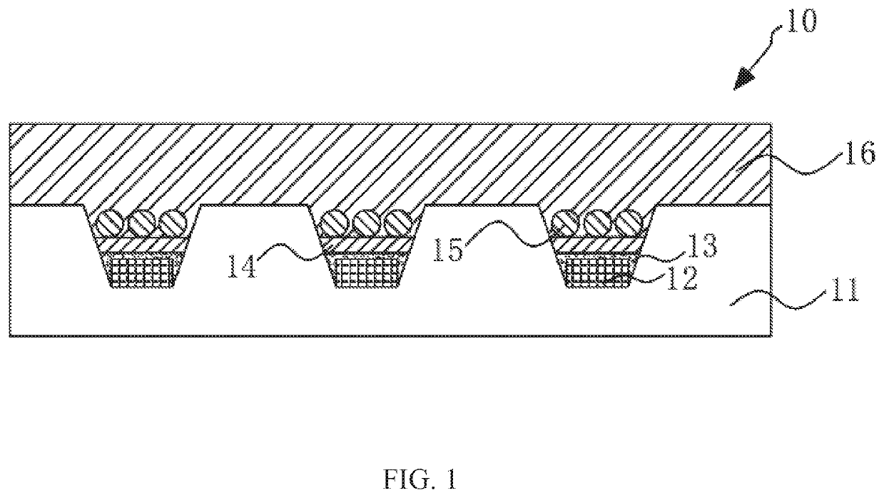
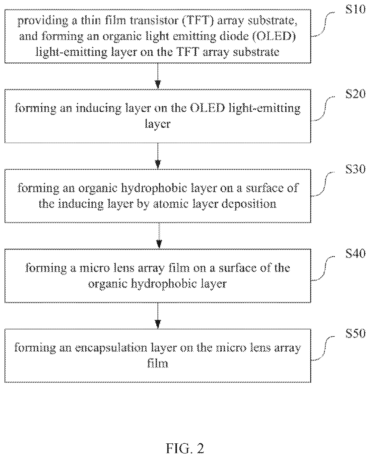
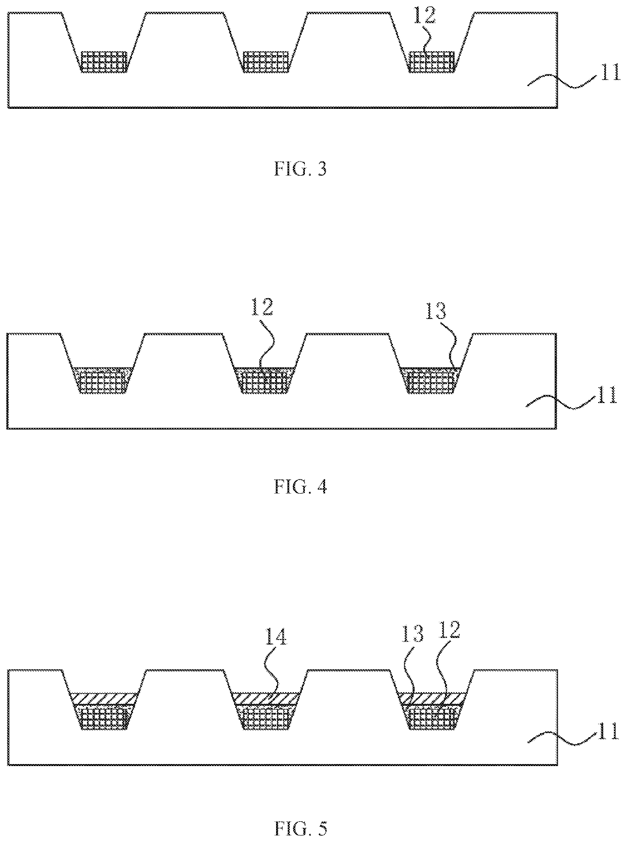
[0035]The following embodiments refer to the accompanying drawings for exemplifying specific implementable embodiments of the present disclosure. Moreover, directional terms described by the present disclosure, such as upper, lower, front, back, left, right, inner, outer, side, etc., are only directions by referring to the accompanying drawings, and thus the used directional terms are used to describe and understand the present disclosure, but the present disclosure is not limited thereto. In the drawings, the same reference symbol represents the same or similar components.

[0036]The invention is directed to an existing OLED display panel. Since a micro lens structure is arranged on an OLED device, the micro lens is usually prepared by using ink jet printing technology, and ink droplets have a relatively large polarity and are printed on a surface of the film with a small contact angle. The surface of the film is easily wetted, which causes the luminous efficiency of the obtained mic...


PUM


Abstract

An organic light emitting diode (OLED) display panel includes a thin film transistor (TFT) array substrate; an OLED light-emitting layer; an encapsulation layer; an inducing layer disposed on a light-emitting side of the OLED light-emitting layer; a micro lens array film disposed over the inducing layer; and an organic hydrophobic layer disposed between the inducing layer and the micro lens array film. By providing the organic hydrophobic layer with strong hydrophobic performance, a surface with a large water contact angle is provided for a subsequent formation of the micro lens array film, thereby improving an optical coupling ratio of the micro lens, and improving luminous efficiency of the OLED light emitting layer.

Description

FIELD OF DISCLOSURE[0001]The present disclosure relates to the field of display technologies, and more particularly to an organic light emitting diode (OLED) display device and a manufacturing method thereof.BACKGROUND[0002]OLED devices have advantages of being light weight, wide viewing angles, fast response times, low temperature resistance, high luminous efficiency, etc., and have received extensive attention in the display field. Especially, OLEDs can be made into flexible displays on flexible substrates, making OLEDs having a broader application prospect. However, light-emitting efficiency of OLED devices is still low, so how to effectively improve the light-emitting efficiency of OLED devices is still a difficult challenge.[0003]Related researches have shown that doping an appropriate amount of small-sized transparent particles in the light penetrating film layer can improve light-emitting efficiency of the film layer. A micro lens technology currently under study is based on ...

Claims


Application Information

Patent Timeline
IPC IPC(8): H01L51/52H01L51/56H01L51/00
CPCH01L51/0005H01L51/56H01L51/5253H01L51/5275H10K59/12H10K50/858H10K71/00H10K50/844H10K71/135
Inventor GUO, TIANFU
Owner WUHAN CHINA STAR OPTOELECTRONICS SEMICON DISPLAY TECH CO LTD
Why Eureka
Try Eureka