Superlattice photodetector/light emitting diode

a photodetector and super-lattice technology, applied in the field of super-lattice photodetector/light-emitting diodes, to achieve the effect of improving current spreading

Active Publication Date: 2020-05-21
ANALOG DEVICES INC
View PDF1 Cites 7 Cited by
  • Summary
  • Abstract
  • Description
  • Claims
  • Application Information

AI Technical Summary

Benefits of technology

[0029]According to another aspect of the present disclosure, a superlattice heterojunction LED with electrical and optical surfaces, wherein optical emitting surface of the substrate is doped to improve current spreading from the ring electrode.

Problems solved by technology

However, there are not corresponding mid-infrared high-brightness LEDs, which might take advantage of this technology base, and there are not corresponding mid-infrared high-brightness LEDs with their own supporting specialized industrial technology base.

Method used


Image

  • Superlattice photodetector/light emitting diode
  • Superlattice photodetector/light emitting diode
  • Superlattice photodetector/light emitting diode

Examples


Embodiment Construction

[0063]The present disclosure relates to light emitting diodes (LEDs). More specifically, this disclosure describes apparatus and techniques relating to the a superlattice structure which functions both as an LED and / or photodiode (PD).

[0064]The following description and drawings set forth certain illustrative implementations of the disclosure in detail, which are indicative of several exemplary ways in which the various principles of the disclosure may be carried out. The illustrative examples, however, are not exhaustive of the many possible embodiments of the disclosure. Other objects, advantages and novel features of the disclosure are set forth in the proceeding in view of the drawings where applicable.

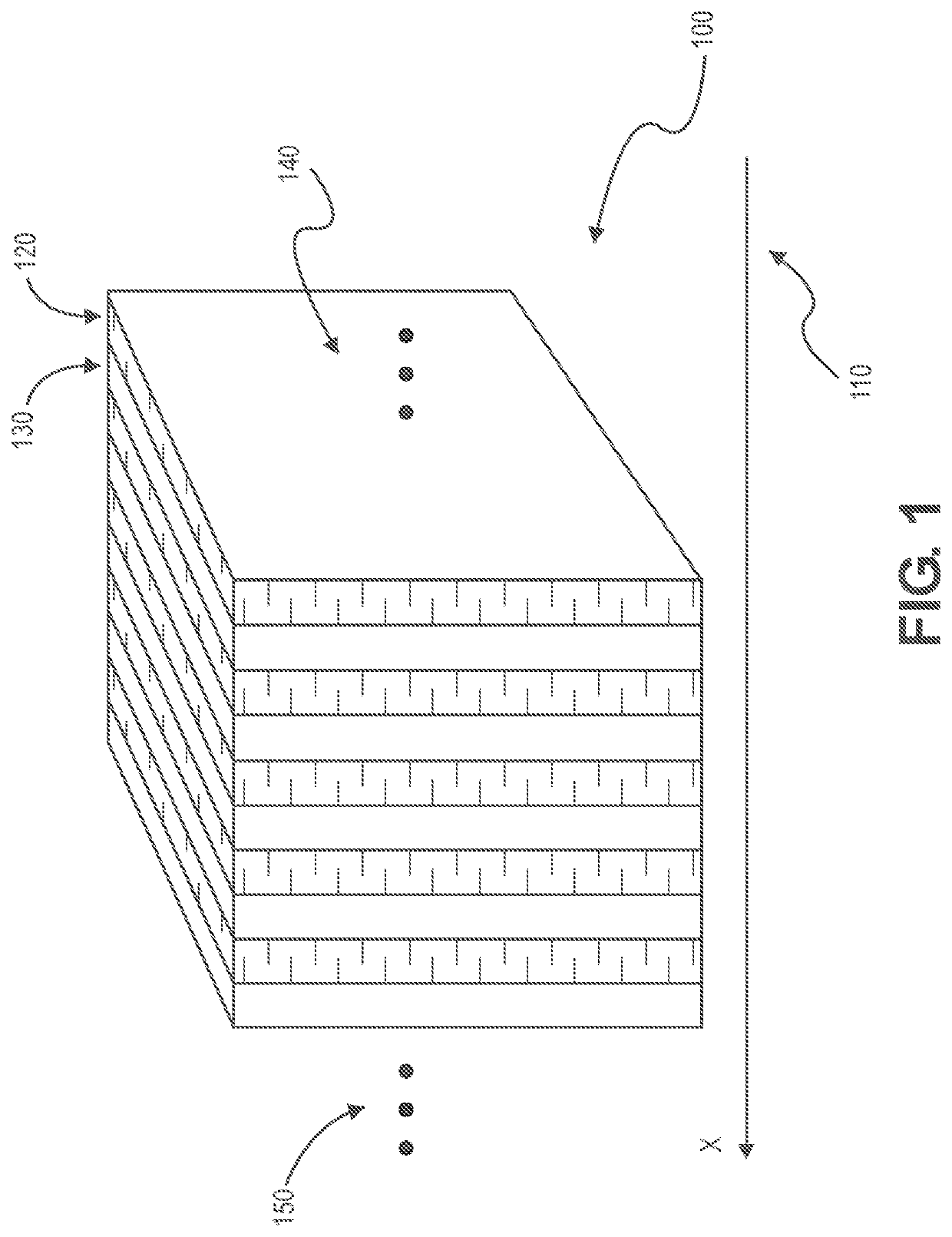
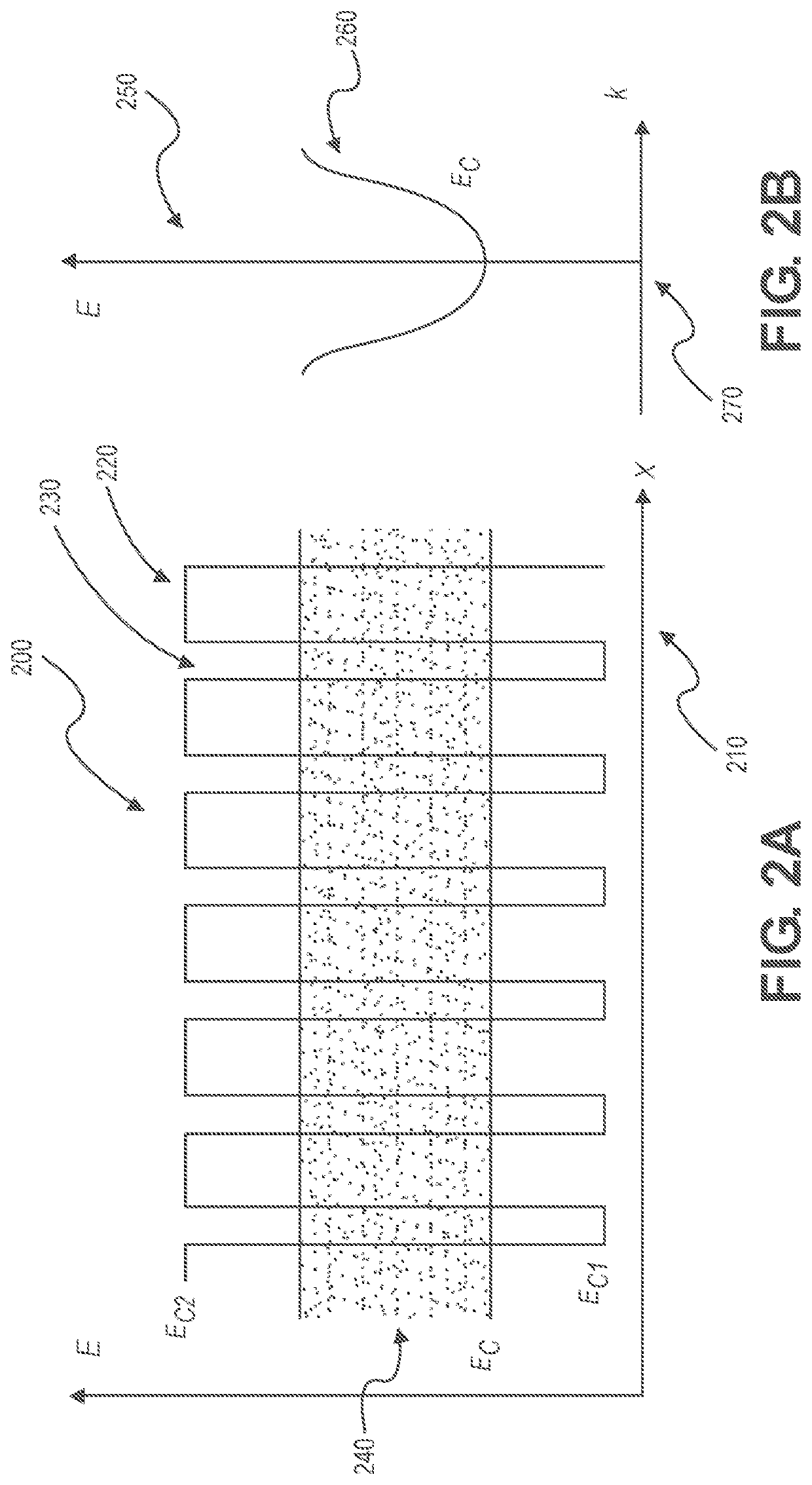
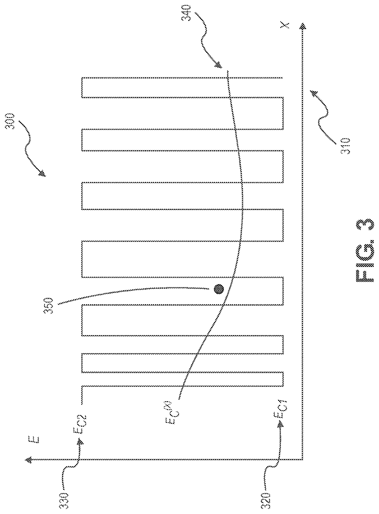
[0065]An IR LED (with wavelength range from 2-15 μm) can be constructed from epitaxial heterostructures of InAs, GaSb, AlSb etc. grown on various substrates such as GaSb, GaAs, or Si. These LEDs typically emit from the “front side”—meaning side closest to the epitaxial growth. A d...


PUM

PropertyMeasurementUnit
wavelength rangeaaaaaaaaaa
thicknessaaaaaaaaaa
thicknessaaaaaaaaaa

Abstract

A device emitting mid-infrared light that comprises a semiconductor substrate of GaSb or closely related material. The device can also comprise epitaxial heterostructures of InAs, GaAs, AlSb, and related alloys forming light emitting structures cascaded by tunnel junctions. Further, the device can comprise light emission from the front, epitaxial side of the substrate.

Description

CROSS-REFERENCE TO RELATED APPLICATION[0001]This application is related to and claims the benefit of priority under 35 U.S.C. § 119(e) to U.S. Provisional Application No. 62 / 770,475 entitled, “SUPERLATTICE PHOTODETECTOR / LIGHT EMITTING DIODE” filed with the U.S. Patent Office on Nov. 21, 2018, which is hereby incorporated by reference in its entirety.FIELD OF THE DISCLOSURE[0002]The present disclosure relates to light emitting diodes (LEDs). More specifically, this disclosure describes apparatus and techniques relating to the a superlattice structure which functions both as an LED and / or photodiode (PD).BACKGROUND[0003]A light-emitting diode (LED) is a two-lead semiconductor light source. It is a p-n junction diode that emits light when activated. When a suitable current is applied to the leads, electrons are able to recombine with electron holes within the device, releasing energy in the form of photons. This effect is called electroluminescence, and the color of the light (correspo...

Claims


Application Information

Patent Timeline
Patent Type & Authority Applications(United States)
IPC IPC(8): H01L33/06H01L33/58H01L33/64H01L31/0352H01L31/0232H01L31/024
CPCH01L31/02327H01L33/06H01L31/024H01L33/58H01L33/644H01L31/035236H01L31/022416H01L33/38H01L33/04H01L2933/0025H01L33/64H01L33/44H01L2933/0058
Inventor DELIWALA, SHRENIKIUTZI, RYAN MICHAEL
Owner ANALOG DEVICES INC
Why Eureka
Try Eureka