
Eureka
For R&D, Eureka makes reading and utilizing patents & technical documents easy.
Eureka AIR
Designed for self-driven R&D workflows. Generate viable solutions, solve complex R&D challenges, empower your innovation with AI.

Eureka Materials
Designed for material experts only. Revolutionize your material R&D, from search, analyze, to developing new materials.

TechResearch
Generate reliable direction feasibility study reports for your R&D in just a few steps.

TechSeek
Discover and master advanced knowledge NOW. Basics, ideas, possibilities, all at once.

TechMind
As an expert in R&D Theories, TechMind can generates customized viable solutions instantly.

TechRisk
Analyze your overall solution with one click, know your potential R&D risks in advance.

TechMonitor
Get weekly tech updates, stay abreast of the latest tech innovations and key insights.
Cu ALLOY BONDING WIRE FOR SEMICONDUCTOR DEVICE
- Summary
- Abstract
- Description
- Claims
- Application Information
AI Technical Summary
Benefits of technology
Problems solved by technology
Method used
Image

Examples
Example
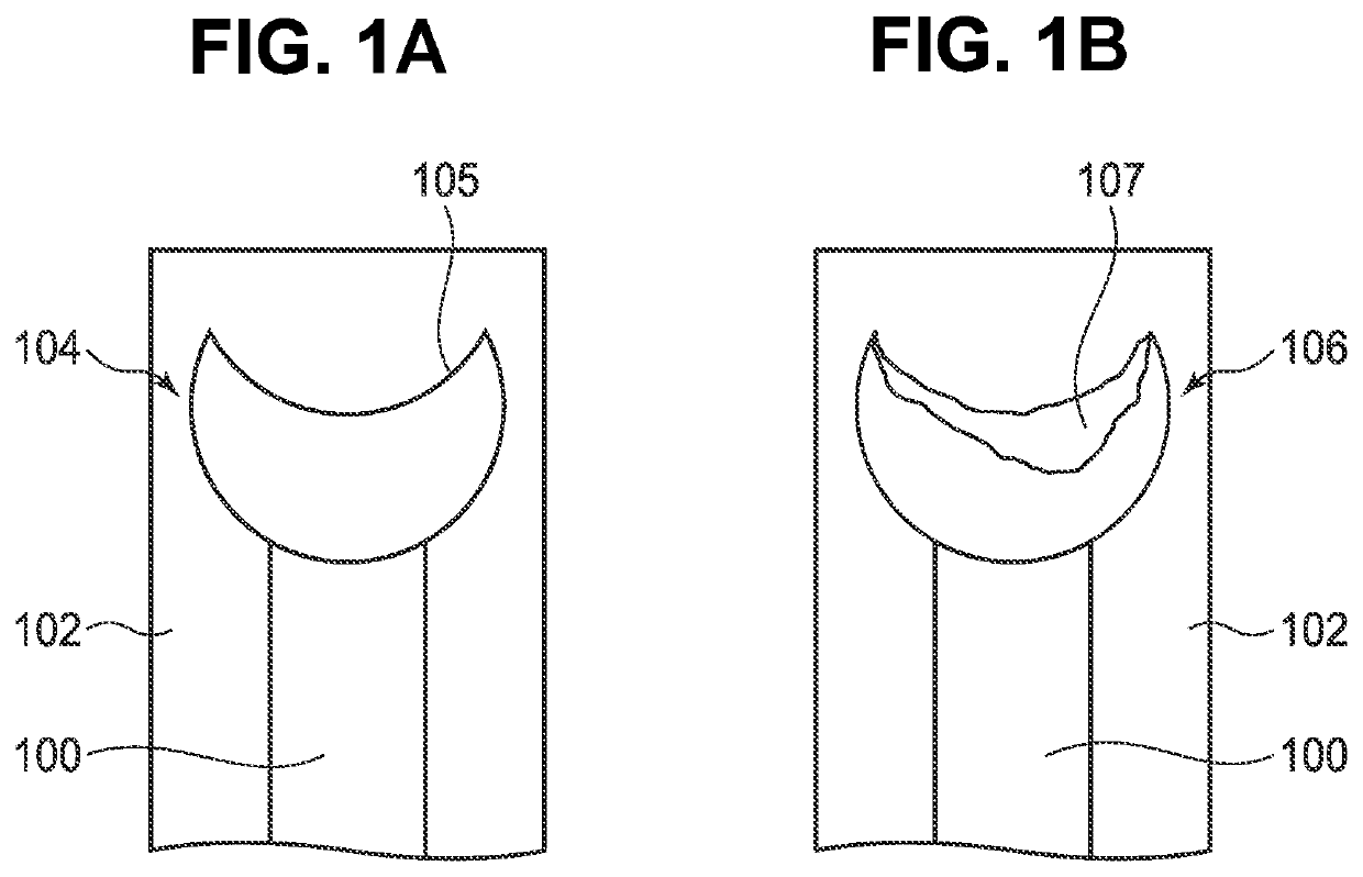
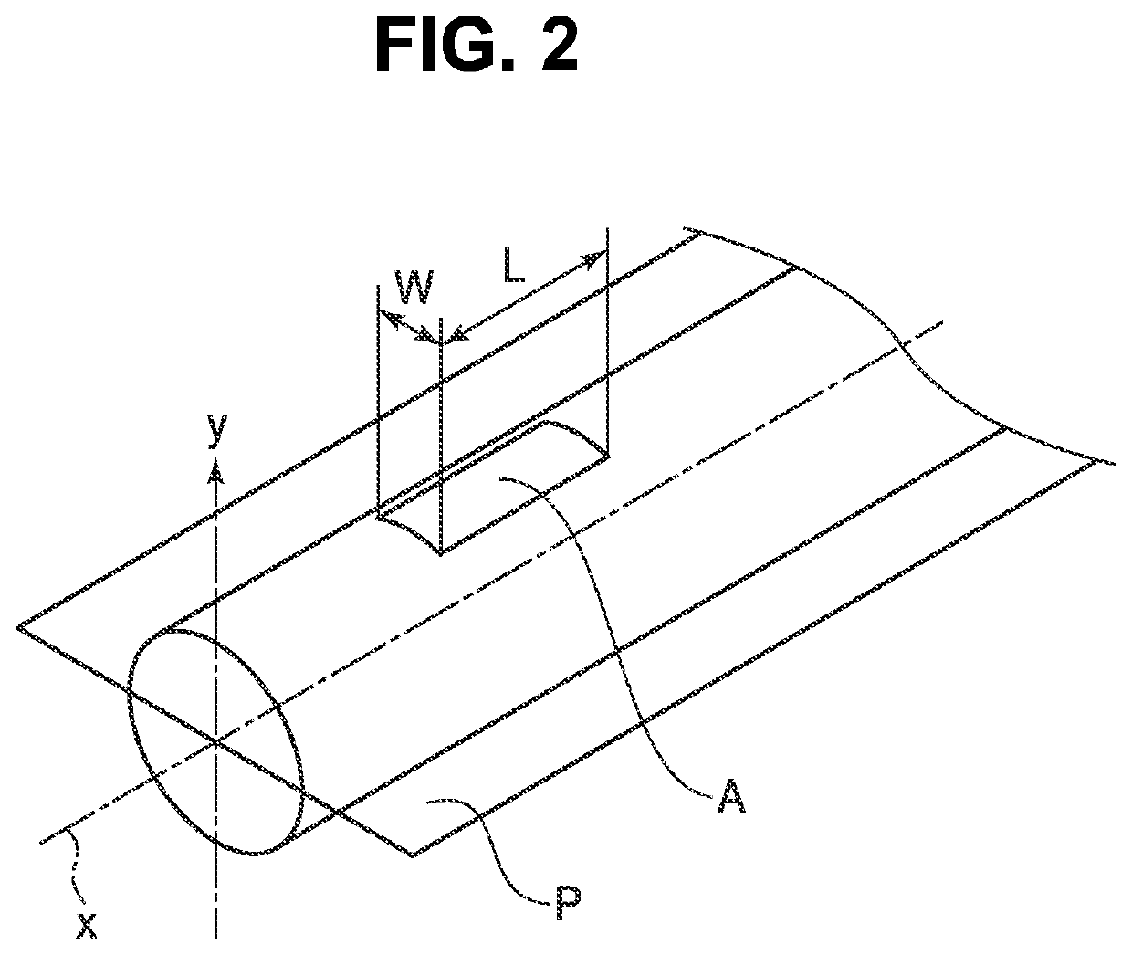
[0079]Examples No. 1 to 94 were alloy bonding wires for a semiconductor device, where the abundance ratio of the crystal orientation having an angular difference of 15 degrees or less from the direction perpendicular to one plane including the wire center axis to the crystal orientations on the wire surface was 25% or more and 70% or less in average area percentage. Thus, all the alloy bonding wires were practicable both in terms of occurrence rate of peelings and occurrence rate of eccentricity. Examples No. 1 to 90, 93, and 94, in which the abundance ratio of the crystal orientation were 30% or more and 70% or less in average area percentage, had no problem in practical use both in terms of occurrence rate of peelings and occurrence rate of eccentricity.
[0080]Examples No. 2, 4 to 10, 12 to 25, 27 to 41, 43 to 46, 48 to 62, 64 to 90, 93, and 94 were Cu alloy bonding wires for a semiconductor device, where the abundance ratio of the crystal orientation having an angular differenc...
PUM
| Property | Measurement | Unit |
|---|---|---|
| Fraction | aaaaa | aaaaa |
| Fraction | aaaaa | aaaaa |
| Fraction | aaaaa | aaaaa |
Abstract
Description
Claims
Application Information
 - R&D Engineer
- R&D Manager
- IP Professional
- Industry Leading Data Capabilities
- Powerful AI technology
- Patent DNA Extraction
Browse by: Latest US Patents, China's latest patents, Technical Efficacy Thesaurus, Application Domain, Technology Topic, Popular Technical Reports.
© 2024 PatSnap. All rights reserved.Legal|Privacy policy|Modern Slavery Act Transparency Statement|Sitemap|About US| Contact US: help@patsnap.com