Semiconductor device

a semiconductor device and semiconductor technology, applied in the field of semiconductor device manufacturing, can solve the problems of high cost, high frequency of replacement and high cost, and the hardness of the substrate is not very high, and achieve the effect of low incidence of electrode continuity failure and resin peeling

Active Publication Date: 2011-01-25
PANNOVA SEMIC
View PDF21 Cites 110 Cited by
  • Summary
  • Abstract
  • Description
  • Claims
  • Application Information

AI Technical Summary

Benefits of technology

[0018]The present invention provides a method for manufacturing a semiconductor device in which, during the partitioning of a substrate having semiconductor layers formed thereon, with gallium contained in at least one of the substrate and the semiconductor layers, partitioning surfaces are formed flat and uniform and the incidence of electrode continuity failures and resin peeling is low.

Problems solved by technology

In case of semiconductor devices utilizing gallium-arsenic, gallium-phosphorus, and similar substrates, the hardness of the substrates is not very high and partitioning is performed by dicing with a dicing saw.
However, in case of substrates utilizing sapphire and gallium nitride, which have a high hardness and are difficult to dice using a dicing saw alone, a technique has been adopted, wherein grooves are formed with a dicing saw along the partitioning locations and the substrate is partitioned by a mechanical action using the grooves as boundaries.
Due to the high hardness of sapphire and gallium nitride, from which substrates in such conventional manufacturing methods are formed, the formation of the grooves used to be a time-consuming task and the blades of the saws used for dicing were heated to elevated temperatures and subjected to intense wear and tear, resulting in a high frequency of replacement and high costs.
The problem was that when cleavage surfaces were non-uniform fracture surfaces, splitting could affect the substrates of the adjacent semiconductor devices.
However, the problem with the conventional method, in which grooves were formed by locally heating a substrate to an elevated temperature of 1000° C. or more by irradiation with a laser beam along partitioning locations and sublimating the gallium-containing compounds utilized in the substrate and the semiconductor layers deposited on the substrate, was that some of the sublimated gallium-containing compounds converted into gallium oxide and other gallium compounds (hereafter called “gallium compounds”) and adhered to the substrate and to the electrodes.
The adhesion of the deposits of gallium compounds to the electrode 5a formed on the substrate caused various problems, such as decreased electrical conduction and reduced wire bond strength when bonding the electrodes of the semiconductor device to other electrodes and in case of wire bonding to other electrodes.
Another problem was that in the case where resin sealing is performed with such deposits still adhered to the substrates, gaps appeared between the substrate and the resin, which allowed moisture to penetrate inside and, upon heating, caused peeling due to interface contamination by the deposits.

Method used


Image

  • Semiconductor device
  • Semiconductor device
  • Semiconductor device

Examples


embodiment 1

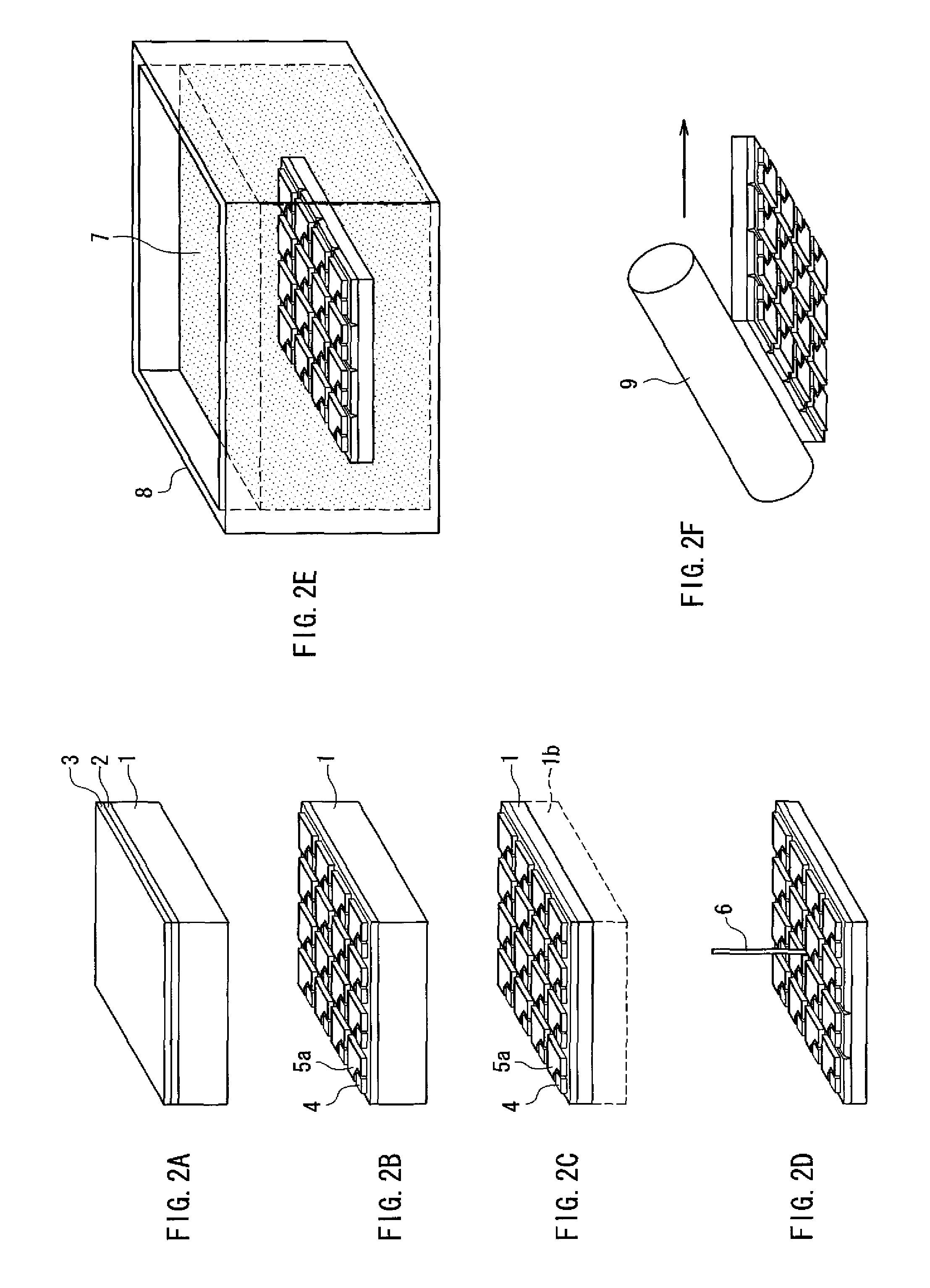
[0040]Explanations regarding a light-emitting element, as an example of the semiconductor devices obtained by the semiconductor device manufacturing method used in Embodiment 1 of the present invention, will be provided with reference to FIGS. 1A-B and FIGS. 2A-F. FIGS. 1A-B illustrate the configuration of a semiconductor device obtained using the semiconductor device manufacturing method used in the embodiments of the present invention. FIGS. 2A-F illustrate a semiconductor device manufacturing method used in an embodiment of the present invention.

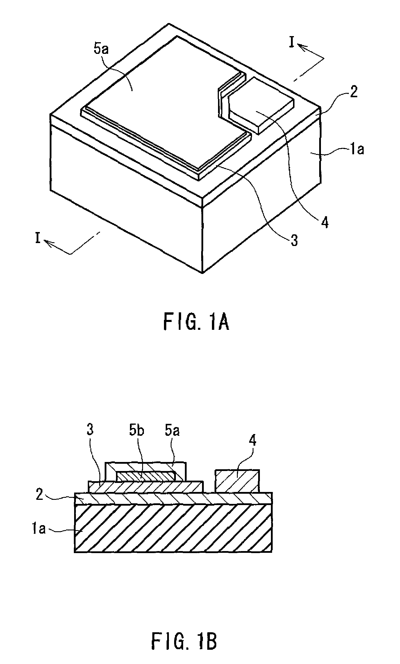
[0041]First of all, explanations will be provided based on FIGS. 1A-B regarding the configuration of a light-emitting element, as an example of the semiconductor devices obtained using the semiconductor device manufacturing method used in the embodiments of the present invention.

[0042]As shown in FIGS. 1A-B, in an individual light-emitting element produced by dicing (length: 350 μm, width: 350 μm, height: 100 μm), an n-type semiconductor ...

embodiment 2

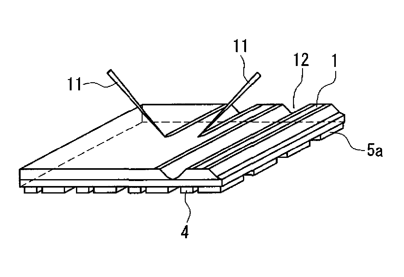
[0061]In the method for manufacturing a semiconductor device used in Embodiment 2 of the present invention, as shown in FIG. 2D, an n-type semiconductor layer 2 and a p-type semiconductor layer 3 are formed on a substrate 1 and grooves are formed by irradiating the face on which the n-type electrode 4 and p-type electrode 5a are formed with YAG laser light 6. However, irradiation with YAG laser light 6 also can be performed on the side opposite the side on which the n-type semiconductor layer 2 and p-type semiconductor layer 3 are formed.

[0062]As shown in FIG. 3A, the grooves 10 were formed by irradiation with the YAG laser light 6 on the side opposite the side where the n-type electrode 4 and p-type electrode 5a were formed. Thus, forming the grooves 10 on the face of the substrate 1 that was opposite the face on which the electrodes were formed made it possible to form the grooves 10 without subjecting the interface between the n-type electrode 4 and p-type electrode 5a and the n-...

embodiment 3

[0067]Next, the method for manufacturing a semiconductor device used in Embodiment 3 of the present invention is explained with reference to FIGS. 4A-H.

[0068]FIGS. 4A-C represent the same steps as FIGS. 2A-C, and therefore the corresponding explanations are omitted. In the steps depicted in FIGS. 4A-C, semiconductor layers and electrodes were formed on a sapphire or gallium nitride substrate, and, in order to separate the substrate 1, which had a predetermined thickness, into individual light-emitting elements, the face of the substrate that was opposite the face on which the p-type electrode 5a and n-type electrode 4 had been formed, was adhered to a dicing tape 13 made of polyethylene etc. (FIG. 4D)

[0069]The face of the substrate 1 on which the p-type electrode 5a and n-type electrode 4 had been formed was irradiated along vertical and horizontal transects with YAG laser light 6 to form boundary grooves with a depth of at least 30% of the thickness of the substrate 1 (FIG. 4).

[007...


PUM

PropertyMeasurementUnit
temperatureaaaaaaaaaa
depthaaaaaaaaaa
heightaaaaaaaaaa

Abstract

The inventive method for manufacturing a semiconductor device is a method for manufacturing a semiconductor device using irradiation with laser light to partition a substrate having semiconductor layers formed thereon, with gallium contained in at least one of the substrate and the semiconductor layers, wherein the method comprises: forming grooves to be used as boundaries between individual substrates by irradiating the substrate along partitioning locations with laser light, immersing the substrate into an acid solution, and partitioning the substrate into individual substrates along the boundaries where grooves are formed. In this manner, it provides a method for manufacturing a semiconductor device in which, during the partitioning of a gallium-containing semiconductor device substrate, deposits of gallium compounds adhered during laser irradiation are removed, partitioning surfaces are formed flat and uniform, and the incidence of electrode continuity failures and resin peeling is low.

Description

[0001]This application is a continuation of U.S. application Ser. No. 11 / 188,601, filed Jul. 25, 2005, pending.BACKGROUND OF THE INVENTION[0002]1. Field of the Invention[0003]The present invention relates to a method for manufacturing a semiconductor device, in which a laser beam is used to dice a substrate having semiconductor layers formed thereon, with gallium contained in at least one of the substrate and the semiconductor layers.[0004]2. Description of Related Art[0005]During the manufacture of light-emitting elements, which are an example of gallium-based semiconductor devices, circuits have to be formed on a wafer used as a substrate and light-emitting elements have to be produced by partitioning the substrate vertically and horizontally.[0006]FIGS. 5A-C illustrates a method for manufacturing light-emitting elements, which are an example of conventional semiconductor devices utilizing substrates on which semiconductor layers are formed, containing gallium.[0007]A substrate 1 ...

Claims


Application Information

Patent Timeline
Patent Type & Authority Patents(United States)
IPC IPC(8): H01L33/00
CPCB23K26/4075B23K26/409H01L33/0095H01L21/78B23K26/40B23K2103/172B23K2103/50
Inventor MAEDA, SYUUSAKU
Owner PANNOVA SEMIC
Why Eureka
Try Eureka