Liquid crystal display device

a liquid crystal display and display device technology, applied in the field of liquid crystal display devices, can solve the problems of poor display image recognition, achieve the effects of reducing light leakage, reducing reflection of external light, and being easy to produ

Active Publication Date: 2020-06-18
SHARP KK
View PDF4 Cites 6 Cited by
  • Summary
  • Abstract
  • Description
  • Claims
  • Application Information

AI Technical Summary

Benefits of technology

[0006]The liquid crystal display device 1R of Comparative Embodiment 1 causes poor recognition of a display image in a bright environment such as an outdoor environment, where the screen reflects excessively. As shown in FIG. 12, this poor recognition is mainly caused by: reflection of the first polarizer 1P surface, interface reflection of the black matrix layer 103 included in the first substrate 100, and interface reflection of the transparent conductive film 1SH that is disposed on a surface of the liquid crystal display device in order to prevent display defect caused by static electricity.
[0008]FIG. 13 is a schematic cross-sectional view of a liquid crystal display device of Comparative Embodiment 2. The liquid crystal display device of Comparative Embodiment 2 can reduce the interface reflection by the above two methods. A liquid crystal display device 1R of Comparative Embodiment 2 has a structure in which the liquid crystal display device 1R of Comparative Embodiment 1 further includes an antireflection film and a λ / 4 plate. In other words, the liquid crystal display device 1R of Comparative Embodiment 2 has the same structure as in the liquid crystal display device 1R of Comparative Embodiment 1 except for including a λ / 4 plate 20 between the transparent conductive film 1SH and the first polarizer 1P and an antireflection film 1RE on the viewing surface side of the first polarizer 1P, as shown in FIG. 13.
[0011]In the liquid crystal display device 1R of Comparative Embodiment 3, the first polarizer 1P and the out-cell retardation layer 21 are used in combination to function as a circularly polarizing plate, which can cut the reflection of the transparent conductive film 1SH and the reflection of the black matrix layer 103. Also, the antireflection film 1RE can cut the reflection of the first polarizer 1P surface. Furthermore, since the slow axis of the out-cell retardation layer 21 and the slow axis of the in-cell retardation layer 22 are perpendicular to each other, at least in the front direction, the out-cell retardation layer 21 and the in-cell retardation layer 22 can cancel out the each other's retardations to achieve a state where the out-cell retardation layer 21 and the in-cell retardation layer 22 substantially do not exist. This structure resultantly provides transmissive display with similar optical properties to those of a typical FFS mode device while achieving low reflection. In the case where a pair of polarizers in the liquid crystal display device are disposed such that their absorption axes form an angle of about 90° when viewed from the viewing surface side, i.e., in the case where the pair of polarizers are arranged in the crossed Nicols, the absorption axes have axial dislocation from the crossed Nicols arrangement when viewed from an oblique direction. In order to correct this axial dislocation, a viewing angle compensation film is generally used in the field of liquid crystal display devices. Although the liquid crystal display device 1R of Comparative Embodiment 3 does not include such a viewing angle compensation film, a viewing angle compensation film may be disposed between the first polarizer 1P and the out-cell retardation layer 21 or between the second polarizer 2P and the second substrate 200.
[0022]JP 2014-186351 A discloses that limiting the range of parameters such as the NZ coefficient of a retardation film including a stretched polymer film achieves a retardation film excellent in driving property, processability, and product reliability. Unfortunately, JP 2014-186351 A discloses no studies about a technique of reducing light leakage in the black display state when viewed from an oblique direction in a liquid crystal display device that includes an in-cell retardation layer, an out-cell retardation layer, and a viewing angle compensation film.
[0023]The present invention has been made under the current situation in the art and aims to provide a liquid crystal display device that is easily producible and is capable of reducing reflection of external light and reducing light leakage in the black display state when viewed from an oblique direction.
[0033]The present invention can provide a liquid crystal display device that is easily producible and is capable of reducing reflection of external light and reducing light leakage in the black display state when viewed from an oblique direction.

Problems solved by technology

The liquid crystal display device 1R of Comparative Embodiment 1 causes poor recognition of a display image in a bright environment such as an outdoor environment, where the screen reflects excessively.

Method used


Image

  • Liquid crystal display device
  • Liquid crystal display device
  • Liquid crystal display device

Examples


embodiment 1

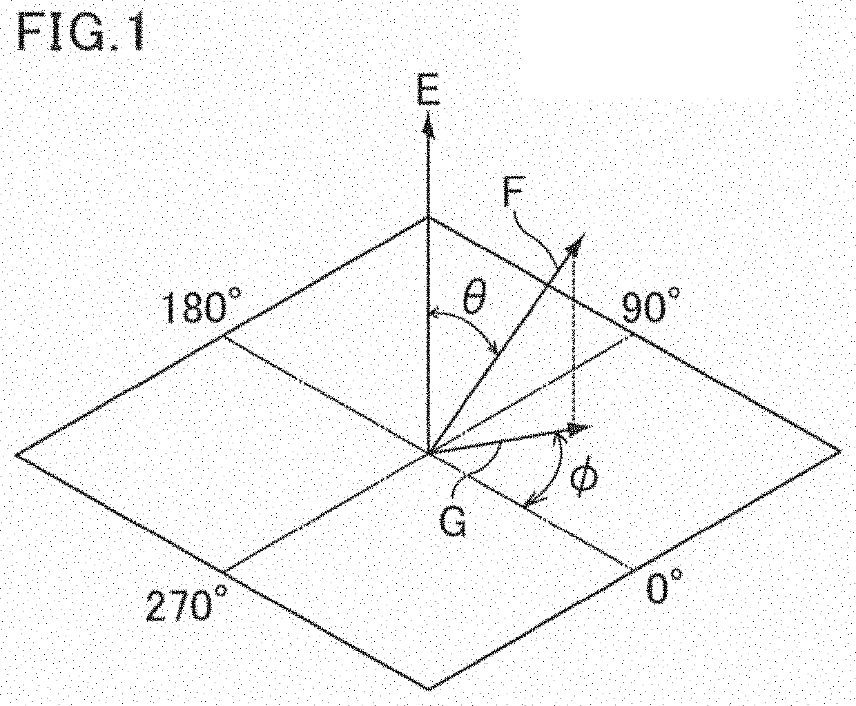
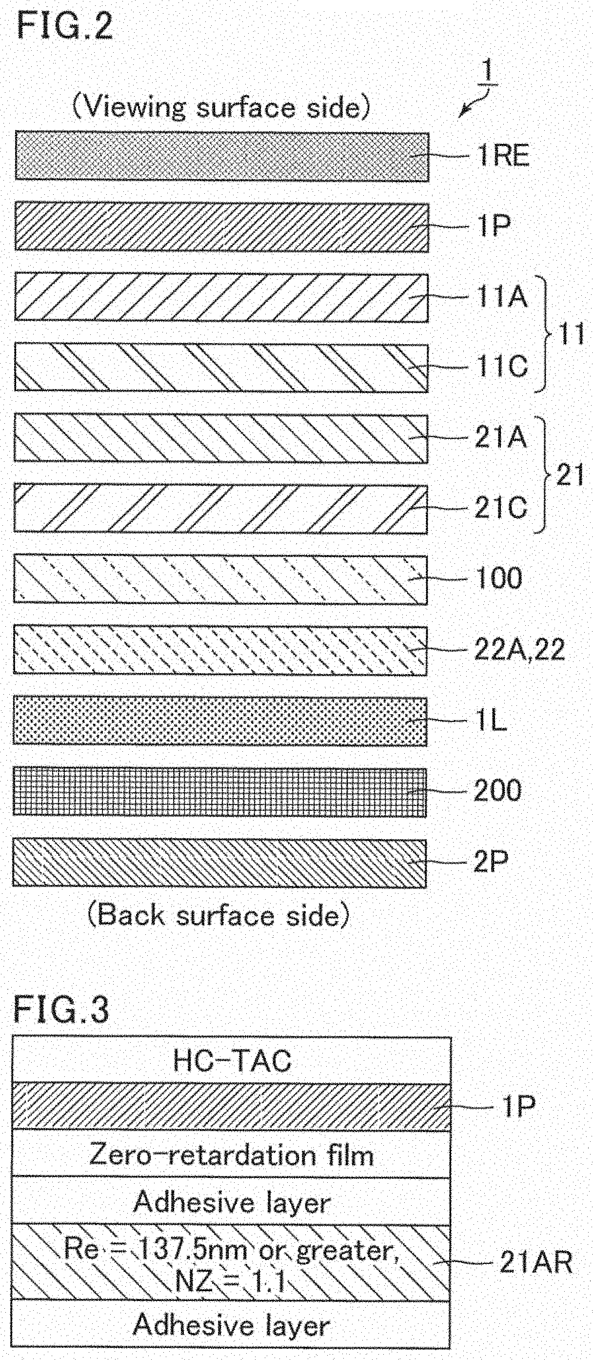
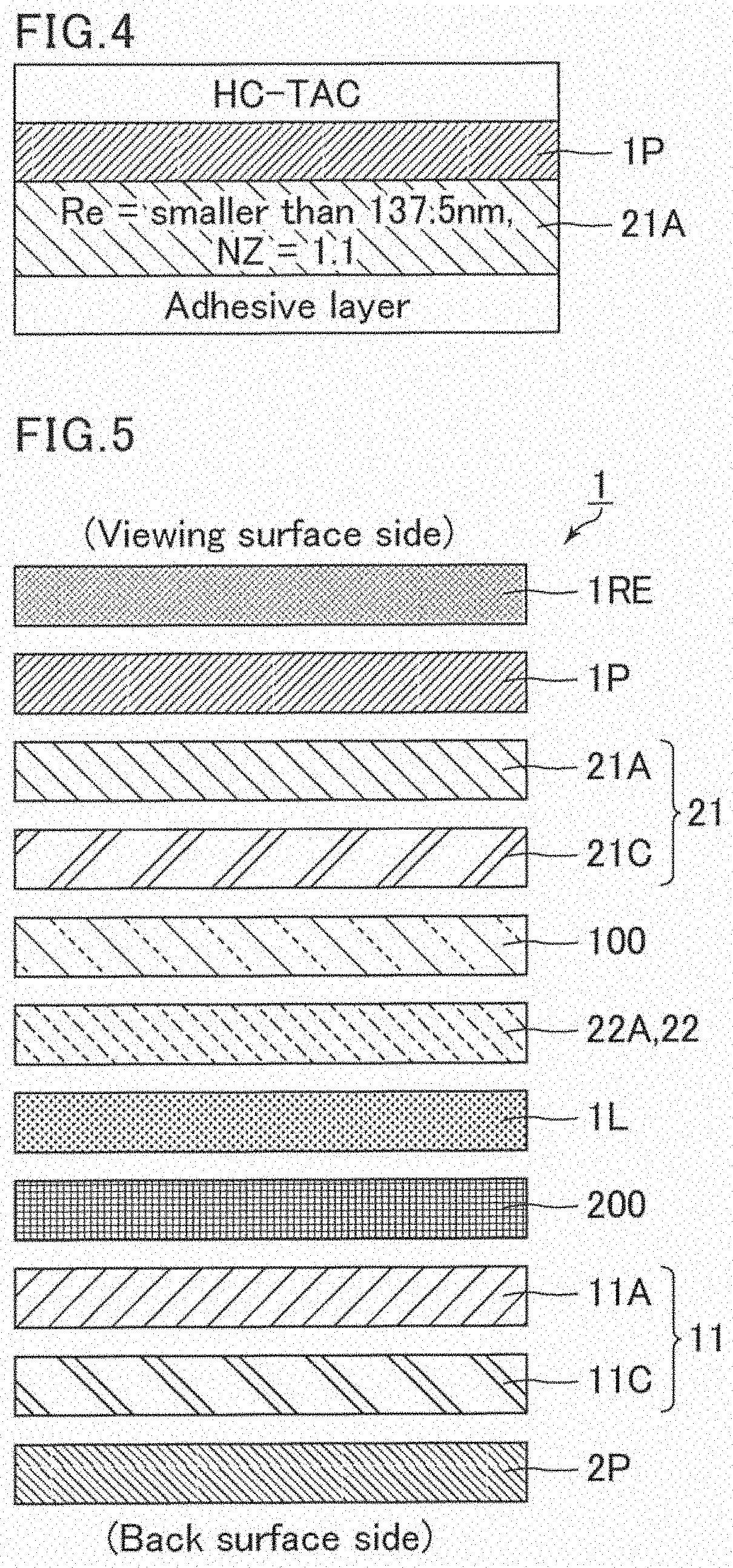
[0071]FIG. 2 is a schematic cross-sectional view of a liquid crystal display device of Embodiment 1. A liquid crystal display device 1 of the present embodiment includes, in the following order from the viewing surface side, a blue antireflection film 1RE as the antireflection film, the first polarizer 1P, the viewing angle compensation layer 11, the out-cell retardation layer 21, the first substrate 100, the in-cell retardation layer 22, the horizontally aligned liquid crystal layer 1L, the second substrate 200, and the second polarizer 2P. The viewing angle compensation layer 11 is a laminate including: the positive A plate 11A as the retardation layer, having an NZ coefficient of 0.7 or greater and 1.3 or smaller and an in-plane retardation of 130 nm or greater and 150 nm or smaller; and the positive C plate 11C as the retardation layer, having an in-plane retardation of 0 nm or greater and 10 nm or smaller and a thickness retardation of 80 nm or greater and 100 nm or smaller, in...

modified example 1 of embodiment 1

[0117]The viewing angle compensation layer 11 of Embodiment 1 may be a laminate (hereinafter, also referred to as a second laminate) including: a first biaxial retardation layer having an NZ coefficient of 1.3 or greater and 1.5 or smaller and an in-plane retardation of 80 nm or greater and 100 nm or smaller; and a second biaxial retardation layer having an NZ coefficient of −1.2 or greater and −0.8 or smaller and an in-plane retardation of 50 nm or greater and 70 nm or smaller, in the stated order from the first polarizer 1P side. The viewing angle compensation layer 11 including the second laminate having a different layer structure from the first laminate is optically equal as a whole to the viewing angle compensation layer 11 including the first laminate.

[0118]The first biaxial retardation layer may be formed by simultaneous biaxial stretching or sequential biaxial stretching a material with a positive birefringence, for example. Specific examples of the material with a positive...

modified example 2 of embodiment 1

[0123]The viewing angle compensation layer 11 of Embodiment 1 may be a laminate (hereinafter, also referred to as a third laminate) including: a third biaxial retardation layer having an NZ coefficient of 1.1 or greater and 1.3 or smaller and an in-plane retardation of 100 nm or greater and 130 nm or smaller; and a fourth biaxial retardation layer having an NZ coefficient of −4.5 or greater and −3.5 or smaller and an in-plane retardation of 10 nm or greater and 30 nm or smaller, in the stated order from the first polarizer 1P side. The viewing angle compensation layer 11 including the third laminate having a different layer structure from the first laminate is optically equal as a whole to the viewing angle compensation layer 11 including the first laminate.

[0124]The third biaxial retardation layer may be formed by the same method as for the first biaxial retardation layer. The fourth biaxial retardation layer may be formed by the same method as for the second biaxial retardation la...


PUM

PropertyMeasurementUnit
thickness retardationaaaaaaaaaa

Abstract

A liquid crystal display device includes sequentially from a viewing surface side: a first polarizer; an out-cell retardation layer; a first substrate; an in-cell retardation layer; a horizontally aligned liquid crystal layer; a second substrate; and a second polarizer. The liquid crystal display device includes a viewing angle compensation film between the first polarizer and the out-cell retardation layer or between the second substrate and the second polarizer. The out-cell retardation layer is a laminate including sequentially from a viewing surface side: a first retardation layer having an NZ coefficient of 1.0-1.1 and an Re of 120 nm or greater and smaller than 137.5 nm; and a second retardation layer having an Re of 0-10 nm and an Rth of 80-150 nm. The in-cell retardation layer is a third retardation layer having an NZ coefficient of 0.7-1.4 and an Re of 120 nm or greater and smaller than 137.5 nm.

Description

CROSS-REFERENCE TO RELATED APPLICATIONS[0001]The present application claims priority under 35 U.S.C. § 119 to U.S. Provisional Application No. 62 / 778,689 filed on Dec. 12, 2018, the contents of which are incorporated herein by reference in their entirety.BACKGROUND OF THE INVENTIONField of the Invention[0002]The present invention relates to liquid crystal display devices. The present invention specifically relates to a liquid crystal display device including a horizontally aligned liquid crystal layer.Description of Related Art[0003]Liquid crystal display devices use a liquid crystal composition for display. According to a typical display mode, voltage is applied to a liquid crystal composition sealed between a pair of substrates to change the alignment of liquid crystal molecules in the liquid crystal composition according to the applied voltage, whereby the amount of light transmitted is controlled. Such liquid crystal display devices have advantageous features such as thin profil...

Claims


Application Information

Patent Timeline
Patent Type & Authority Applications(United States)
IPC IPC(8): G02F1/13363G02B5/30G02F1/1335
CPCG02F2001/133541G02F1/133634G02F1/133528G02B5/3083G02F1/13363G02F2413/03G02F2413/04G02F1/133638G02F1/133738G02F1/133541
Inventor HASEGAWA, MASAHIROSAKAI, AKIRAKOIDE, TAKAKOKAWAHIRA, YUICHIMURATA, KOJIMINOURA, KIYOSHI
Owner SHARP KK
Why Eureka
Try Eureka