Composition for semiconductor surface treatment and treatment method of semiconductor surface

Inactive Publication Date: 2020-07-02
JSR CORPORATIOON
View PDF0 Cites 0 Cited by
  • Summary
  • Abstract
  • Description
  • Claims
  • Application Information

AI Technical Summary

Benefits of technology

The patent text describes a composition and method for treating semiconductor surfaces to remove contaminants and protect metal wiring materials during polishing and cleaning processes. The composition is effective in reducing damage to the surface and minimizing impurities, resulting in a higher quality semiconductor surface.

Problems solved by technology

However, even when the pH of the composition for semiconductor substrate cleaning is adjusted to be high, it is difficult to suppress damage to the metal wiring material and the like only by the addition of polyethyleneimine or alkanolamine.

Method used


Image

  • Composition for semiconductor surface treatment and treatment method of semiconductor surface
  • Composition for semiconductor surface treatment and treatment method of semiconductor surface
  • Composition for semiconductor surface treatment and treatment method of semiconductor surface

Examples


Embodiment Construction

[0020]Hereinafter, embodiments of the disclosure will be described in detail. Moreover, the disclosure is not limited to the following embodiments and also include various modifications implemented in the range in which the spirit of the disclosure is not changed.

[0021]An aspect of the composition for semiconductor surface treatment according to the disclosure contains:

[0022](A) a compound represented by the following Formula (1); and

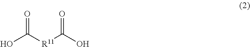
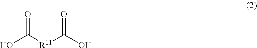
[0023](B) a compound represented by the following Formula (2).

R1—L1—R2   (1)

[0024](in Formula (1), R1 represents a linear or branched alkyl group having 6 to 18 carbon atoms, R2 represents an organic group having 2 or more and 5 or less nitrogen atoms, and L1 represents a single bond or a divalent linking group).

[0025](in Formula (2), R11 represents an organic group having 1 to 12 carbon atoms).

[0026]In an aspect of the composition for semiconductor surface treatment, R2 in the compound represented by Formula (1) may be a group represented by the follow...


PUM

PropertyMeasurementUnit
Temperatureaaaaaaaaaa
Compositionaaaaaaaaaa
Solubility (mass)aaaaaaaaaa

Abstract

Provided are a composition for semiconductor surface treatment capable of effectively diminishing or removing contaminations from a semiconductor surface and suppressing damage to a metal wiring material and the like when being used in treatments such as polishing and cleaning and a treatment method of a semiconductor surface using the composition. The composition for semiconductor surface treatment according to an embodiment of the disclosure contains (A) a compound represented by the following Formula (1) and (B) a compound represented by the following Formula (2):R1—L1—R2   (1)(in Formula (1), R1 represents a linear or branched alkyl group having 6 to 18 carbon atoms, R2 represents an organic group having 2 or more and 5 or less nitrogen atoms, and L1 represents a single bond or a divalent linking group)(in Formula (2), R11 represents an organic group having 1 to 12 carbon atoms).

Description

CROSS-REFERENCE TO RELATED APPLICATIONS[0001]This application claims the priority benefit of Japanese Patent Application No. 2018-242423, filed on Dec. 26, 2018. The entirety of the above-mentioned patent application is hereby incorporated by reference herein and made a part of this specification.BACKGROUND OF THE DISCLOSURETechnical Field[0002]The disclosure relates to a composition for semiconductor surface treatment and a treatment method of a semiconductor surface using the same.Related Art[0003]Chemical mechanical polishing (CMP) has been widely used in the planarization technology in the manufacture of semiconductor devices. The slurry for chemical mechanical polishing used in CMP contains an etching agent and the like in addition to grinding particles (abrasive grains). Moreover, in the manufacture of semiconductor devices, it is required to remove contaminations such as polishing scraps and organic residues from the surface of the semiconductor substrate after CMP, and clean...

Claims


Application Information

Patent Timeline
IPC IPC(8): C09K13/00H01L21/3213
CPCH01L21/32134C09K13/00C11D3/3723C11D3/2082C11D3/2086C11D3/30C11D3/32C11D3/33C11D1/90C11D1/10C11D1/88H01L21/02074C11D2111/22C09G1/04C23F1/38C23F3/00C09G1/02H01L21/30625H01L21/3212C09K13/02
Inventor MITSUMOTO, KIYOTAKASATO, KEISUKEKUBOTA, KIYONOBU
Owner JSR CORPORATIOON
Why Eureka
Try Eureka