

Pseudo static random access memory and method for operating pseudo static random access memory
a random access memory and pseudo-static technology, applied in static storage, information storage, digital storage, etc., can solve problems such as inconstant read latency, increased current consumption, and possible bus conflict problems, so as to prevent bus conflict
- Summary
- Abstract
- Description
- Claims
- Application Information
AI Technical Summary
Benefits of technology
Problems solved by technology
Method used
Image

Examples
first embodiment
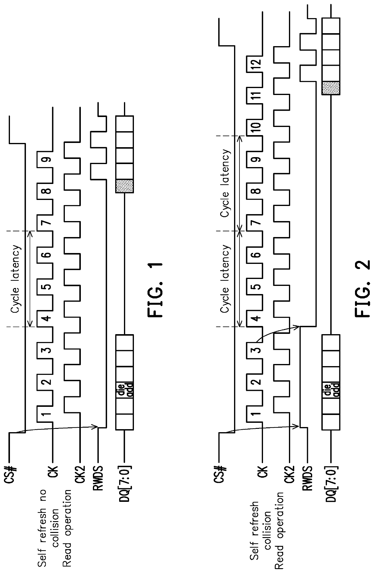
[0036]FIG. 6 is a diagram illustrating signal timing sequences of the memory chips according to the disclosure. The first memory chip 110_0 is selected to perform a read operation, and no self refresh collision occurs in the first memory chip 110_0. The second memory chip 110_1 is not selected, i.e. in a standby state, while a self refresh collision occurs in the second memory chip 110_1. The read latency of the first memory chip 110_0 is set to be a fixed period (for example, two units of cycle latency) that self refresh operation is allowed to be completed.
[0037]In the present embodiment, a chip address is input at a rising edge of a second clock of a clock signal CK, and is marked as “die add” in the data signal DQ [7:0]. A portion marked by oblique lines in the data signal DQ [7:0] indicates that data is read out. In addition, when the control signal CS# changes from a high level to a low level, the first memory chip 110_0 outputs an RWDS signal at a high level. At the same time...
second embodiment
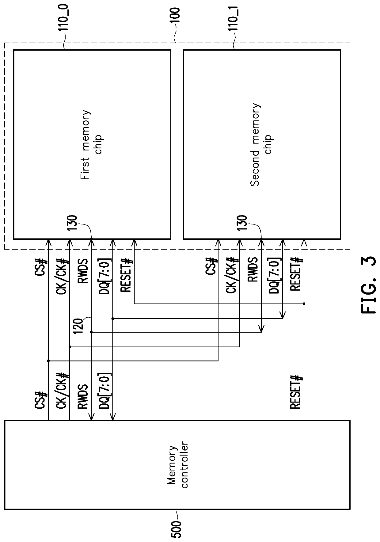
[0040]Therefore, according to a method for operating the memory chips of the second embodiment, even if these memory chips have different operating speeds, the problem of the bus conflict may also be avoided between the first memory chip 110_0 and the second memory chip 110_1.
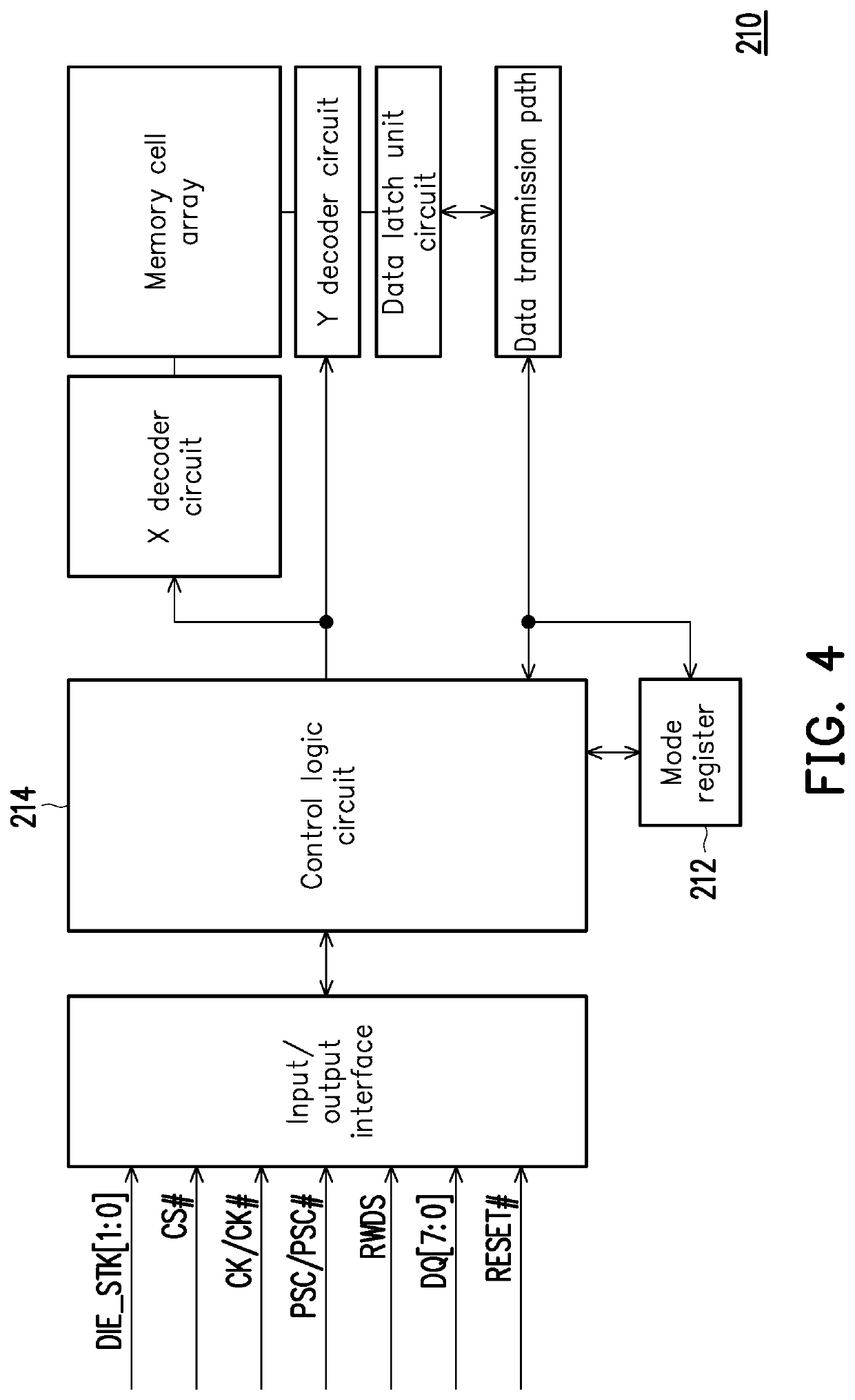
[0041]FIG. 8 is a schematic general diagram illustrating a signal generation circuit according to one embodiment of the disclosure. FIG. 9 is a schematic diagram illustrating an internal part of the signal generation circuit of the embodiment of FIG. 8. Referring to FIG. 8 and FIG. 9, the signal generation circuit 400 is, for example, arranged in the control logic circuit 214 in FIG. 4 or FIG. 5. In one embodiment, the signal generation circuit 400 may also be arranged in other circuit blocks of the memory chips 210 and 310.
[0042]In the present embodiment, the signal generation circuit 400 includes an output control circuit 410, a latency circuit 420, an RWDS signal control circuit 430, a read latency determina...
third embodiment
[0053]Therefore, even if these memory chips have different operating speeds, the problem of the bus conflict may also be avoided between the first memory chip 110_0 and the second memory chip 110_1.
[0054]FIG. 12 is a diagram illustrating signal timing sequences of the memory chips according to a fourth embodiment of the disclosure. A main difference between the fourth embodiment and the third embodiment is that the first memory chip 110_0 has a lower operating speed. In the present embodiment, before the falling edge of the third clock of the internal clock signal CK0 of the first memory chip 110_0, the RWDS signal of the first memory chip 110_0 changes to a low level. For example, in response to a rising edge of the third clock of the internal clock signal CK0, the RWDS signal of the first memory chip 110_0 changes to a low level. The rising edge of the third clock of the internal clock signal CK0 is earlier than a rising edge of a fourth clock of the clock signal CK. That is, bef...
PUM
 Abstract
Description
Claims
Application Information