Imaging optical device and manufacturing method therefor

a manufacturing method and optical device technology, applied in the field of optical lenses, can solve the problems of reducing the connection strength and reliability affecting the quality of the imageable optical device, so as to reduce the influence of the subsequent manufacturing process, the effect of reducing the amount of adjustmen

Pending Publication Date: 2020-12-31
NINGBO SUNNY OPOTECH CO LTD
View PDF0 Cites 7 Cited by
  • Summary
  • Abstract
  • Description
  • Claims
  • Application Information

AI Technical Summary

Benefits of technology

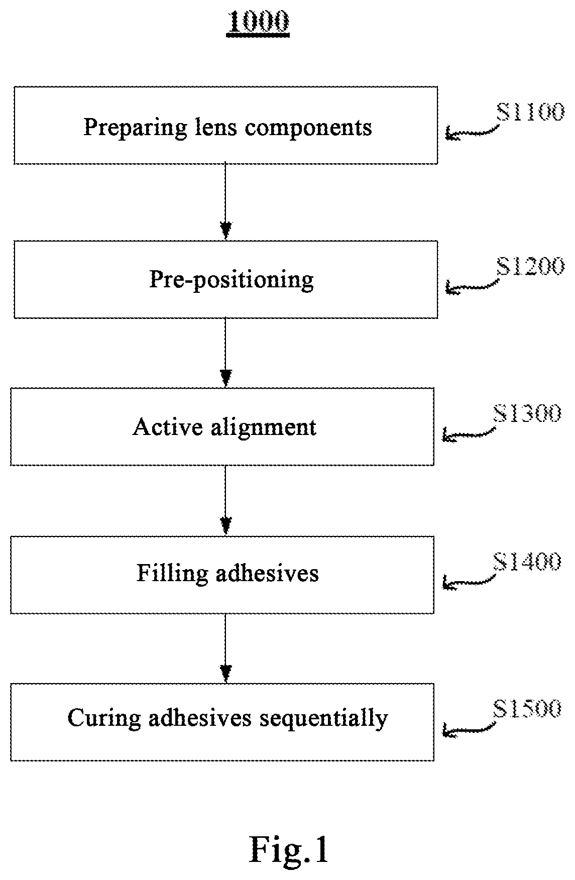
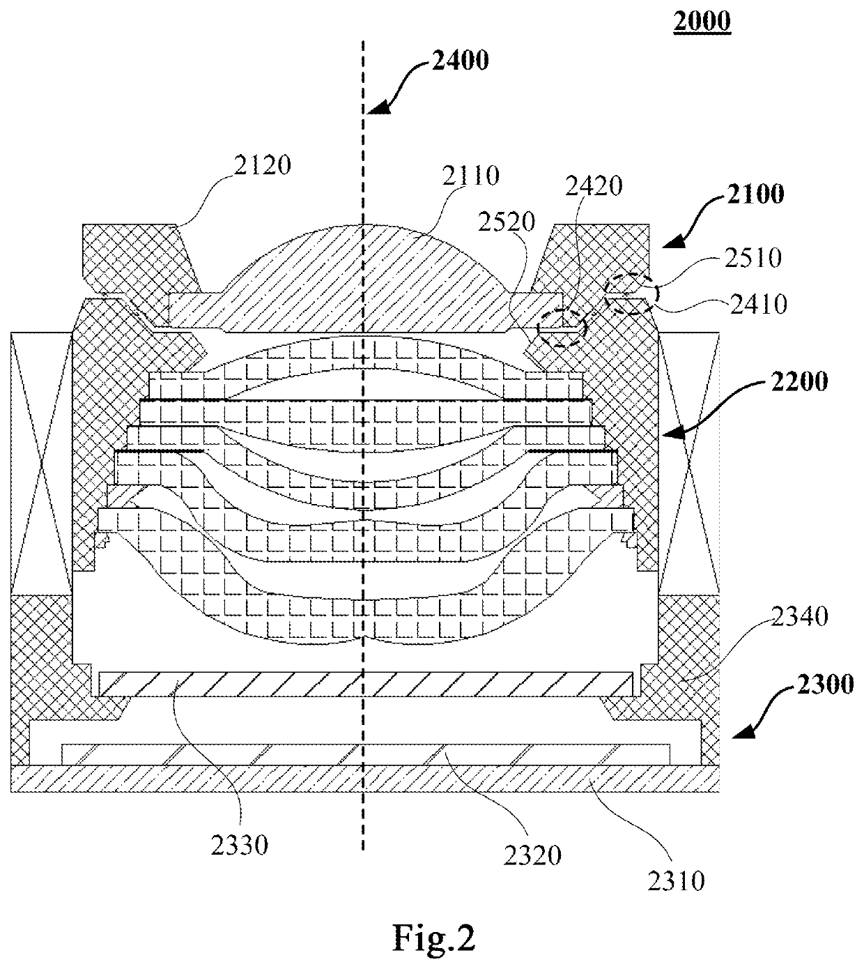
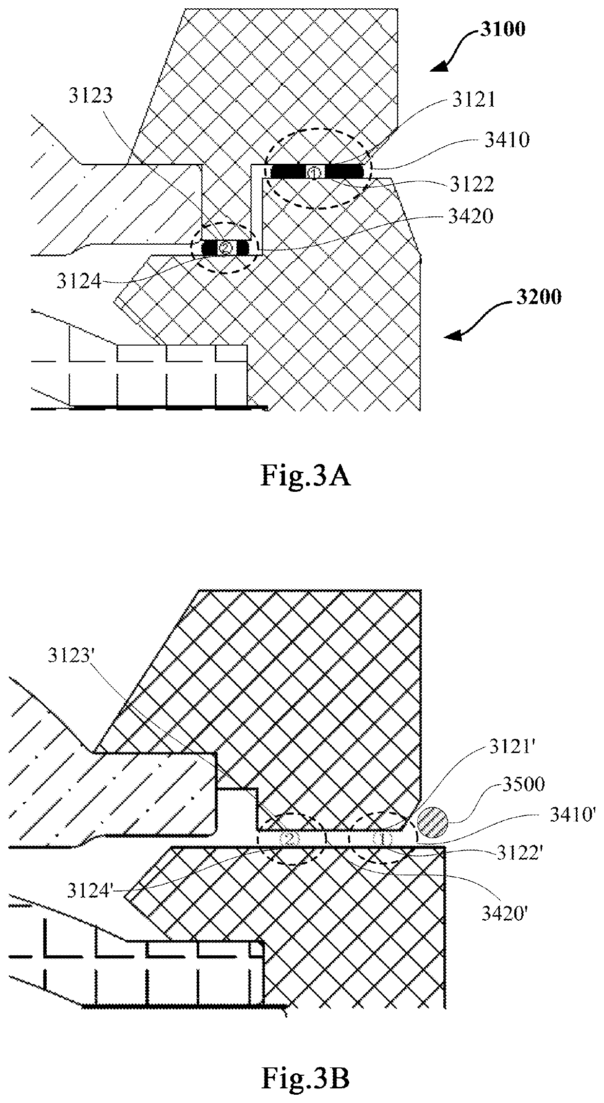
[0074]According to the technical solution provided by the present application, the imageable optical device is assembled by a plurality of lens components separated from each other, and the adjustment amount can be provided by using the first adhesive and the second adhesive for adjusting the relative positions of two adjacent lens components. Since the first adhesive and the second adhesive can be cured sequentially, on one hand, the imageable optical device may be pre-fixed by the firstly cured first adhesive to reduce the influence of the subsequent manufacturing process on the imageable optical device; and on the other hand, a connection strength and reliability of the imageable optical devices can be increased by the subsequently cured second adhesive.
[0075]In addition, compared with the prior art, the technical solution of the present application at least achieves the following beneficial effects: by adding an air escape channel design (for example, air escape holes, grooves, air escape grooves, etc.) to the lens module, the baking variation of the lens module is reduced, thereby avoiding adverse effects on the reliability of the module due to the heat-expansion or cold-contraction of the air during the baking process.

Problems solved by technology

Factors affecting resolution of the imageable optical devices of a given optical design include quality of the optical imaging lens and manufacturing errors in the process of module encapsulation.
Particularly, in the manufacturing process of the optical imaging lens, factors affecting the resolution of the lens come from: the errors of each element and its assembly, the error of the thickness of the lens spacer element, the error of the assembly of each lens, and the change of the refractive index of lens material, etc.
Among them, the errors of each element and its assembly include: the errors of the thickness of the optical surface of each lens unit, the rise of the optical surface of the lens, the shape of the optical surface, the radius of curvature, the eccentricity of the single side and the eccentricity between the surfaces of the lens, and the inclination of the optical surface of the lens.
The thickness error of the lens spacer element depends on the processing accuracy of the element.
The error of the assembly of each lens depends on the dimensional tolerance of the assembled components and the assembly accuracy of the lens.
The error introduced by the change of the refractive index of the lens material depends on the stability of the material and batch consistency.
The errors of the above-mentioned components affecting the resolution produce a cumulative deterioration, and this cumulative error will continue to increase as the number of lens increases.
However, since the lens with high pixels and large aperture is more sensitive, it requires strict tolerances, for example, 1 μm of lens eccentricity for some sensitive lens will cause 9′ inclination of the image plane, thereby making lens processing and assembly more and more difficult.
At the same time, due to the long feedback cycle in the assembly process, the process capability index (CPK) of lens assembly is low and fluctuates greatly, resulting in high defective rate.
And as mentioned above, since there are many factors affecting the resolution of the lens, and they exist in multiple components, the control of each factor has the limit of manufacturing accuracy.
If only the accuracy of each component is improved, the improvement ability is limited, and the improvement cost is high; and it still cannot meet the increasing demand of the market for image quality.
On the other hand, during the processing of imageable optical devices, the assembly process of various structural components (e.g., the mounting of photosensitive chip, the process of locking and attaching the motor and the lens, etc.) may cause inclination of the photosensitive chip; the superposition of multiple inclinations may cause the resolution of the imaging module to fail to meet the established specifications, and thereby cause the low yield of the module factory.
However, this process has limited compensation capability, since various aberrations affecting the resolution come from the capability of the optical system itself, when the resolution of the optical imaging lens itself is insufficient, the existing active alignment process of the photosensitive module is difficult to compensate.
On the other hand, the lens is an important component of the camera module, which directly affects the imaging quality of the camera module.
Since air between the upper and lower lens components will cause gas expansion during baking, the gas expansion will influence the upper and lower lens components, thereby changing the relative positions of the optical elements of the lens components, resulting in a decrease in optical capability.
Therefore, how to avoid the influence of air on the camera module during the baking process is a problem to be solved in this field.

Method used


Image

  • Imaging optical device and manufacturing method therefor
  • Imaging optical device and manufacturing method therefor
  • Imaging optical device and manufacturing method therefor

Examples


first embodiment

[0163]FIG. 10 is a cross-sectional view showing a first air escape channel 5010 of an optical lens 10 according to the present application.

[0164]According to the first embodiment of the present application, the first escape channel 5010 may be: an air escape hole arranged in the first lens barrel 104 in a direction parallel to the optical axis of the optical system consisting of the first lens and the second lens (for example, the vertical direction as shown in FIG. 10), or arranged in the first lens barrel 104 at an angle relative to the direction.

[0165]As shown in FIG. 10, for example, the first air escape channel 5010 may be vertically arranged in the first lens barrel 104. One end 512 (bottom) of the first air escape channel 5010 leading to the cavity 1200 is arranged with a relatively large opening to prevent adhesive from overflowing from the inside to block the air escape hole; the other end 514 of the first air escape channel 5010 leads to the outside, so that an internal sp...

second embodiment

[0166]FIG. 11 is a cross-sectional view showing a second air escape channel 5020 of an optical lens 20 according to the present application.

[0167]According to the second embodiment of the present application, the second air escape channel 5020 may be: an air escape hole arranged in the first lens barrel 104 in a direction perpendicular to the optical axis of the optical system consisting of the first lens and the second lens (for example, the horizontal direction as shown in FIG. 11), or arranged in the first lens barrel 104 at an angle relative to the direction.

[0168]As shown in FIG. 11, for example, the second air escape channel 5020 may be horizontally arranged in the first lens barrel 104. One end 522 of the second air escape channel 5020 leading to the cavity 1200 is arranged with a relatively large opening to prevent adhesive from overflowing from the inside to block the air escape hole; the other end 524 of the second air escape channel 5020 leads to the outside, so that an i...

third embodiment

[0169]FIG. 12 is a cross-sectional view showing a third air escape channel 5030 of an optical lens 30 according to the present application.

[0170]According to the third embodiment of the present application, the third air escape channel 5030 may be: an air escape hole arranged in the ineffective area of the first lens 102 in a direction parallel to the optical axis of the optical system consisting of the first lens and the second lens, or arranged in the ineffective area of the first lens 102 at an angle relative to the direction. As explained above, the ineffective area of the first lens 102 represents the outer edge of the first lens 102 not involved in imaging. However, it should be understood that the ineffective area herein is only an example, and it may not be arranged on the outer circumference of the lens or have other configurations as long as it does not affect the imaging.

[0171]As shown in FIG. 12, for example, the third air escape channel 5030 may be vertically arranged i...


PUM

PropertyMeasurementUnit
widthaaaaaaaaaa
widthaaaaaaaaaa
shapeaaaaaaaaaa

Abstract

A manufacturing method of an imageable optical device includes pre-positioning at least two lens components along the optical axis so that the at least two lens components are able to form an image. A first structural gap and a second structural gap are arranged at different positions between two adjacent lens components. The method also includes adjusting relative positions of the pre-positioned at least two lens components by active alignment, arranging a first adhesive in the first structural gap, arranging a second adhesive in the second structural gap, and sequentially curing the first and second adhesives. The influence of later steps of the manufacturing process on the imageable optical device may thus be reduced, and connection strength and reliability of the imageable optical device are improved by subsequently curing the second adhesive. Also provided are an optical lens having an air escape channel, and an assembly method thereof.

Description

CROSS REFERENCE[0001]This application claims priorities of invention patent application No. 201810219941.2 filed with the Chinese Patent Office on Mar. 16, 2018, titled “Imageable Optical Device and Manufacturing Method Thereof”; utility model patent application No. 201820362456.6 filed with the Chinese Patent Office on Mar. 16, 2018, titled “imaginable optical device”; and invention patent application No. 201810220345.6 filed with the Chinese Patent Office on Mar. 16, 2018, titled “Optical Lens with Air Escape Channel and Assembly Method Thereof”; and utility model patent application No. 201820366562.1 filed with the Chinese Patent Office on Mar. 16, 2018, titled “Optical Lens and Camera Module”; the entire content of the above patent applications is incorporated herein by reference.TECHNICAL FIELD[0002]This application relates to field of optical lens, and particularly, to an imageable optical device and manufacturing method thereof, solutions for optical lens and camera module, a...

Claims


Application Information

Patent Timeline
Patent Type & Authority Applications(United States)
IPC IPC(8): G02B7/00G02B7/02
CPCG02B7/021G02B7/025G02B7/003G02B7/02
Inventor JIANG, HENGCHU, SHUIJIALIU, LINZHENG, CHENGCHANG
Owner NINGBO SUNNY OPOTECH CO LTD
Why Eureka
Try Eureka