Supercharge Your Innovation With Domain-Expert AI Agents!

Image processing circuit and associated image processing method

a processing circuit and image technology, applied in image enhancement, image analysis, instruments, etc., can solve the problems of original texture of image and affect display quality, and achieve the effect of improving image sharpness and preventing the appearance of conventional defects in the output imag

Active Publication Date: 2021-01-28
REALTEK SEMICON CORP
View PDF0 Cites 0 Cited by
  • Summary
  • Abstract
  • Description
  • Claims
  • Application Information

AI Technical Summary

Benefits of technology

The technical effect of this patent is to provide an image processing circuit that improves image sharpness without causing conventional defects in the output image. This solves the problem of the conventional problem.

Problems solved by technology

However, when the frequency of the linear HPF is high (or the length of the HPF is short), the original texture of the image will be damaged, resulting in that the edge luminance of an object is higher than its central luminance.
In addition, when the frequency of the linear HPF is low (or the length of the HPF is long), the sharpened object becomes thicker and a thicker ringing is formed at the edge of the object, which affects the display quality.

Method used


Image

  • Image processing circuit and associated image processing method
  • Image processing circuit and associated image processing method
  • Image processing circuit and associated image processing method

Examples


Embodiment Construction

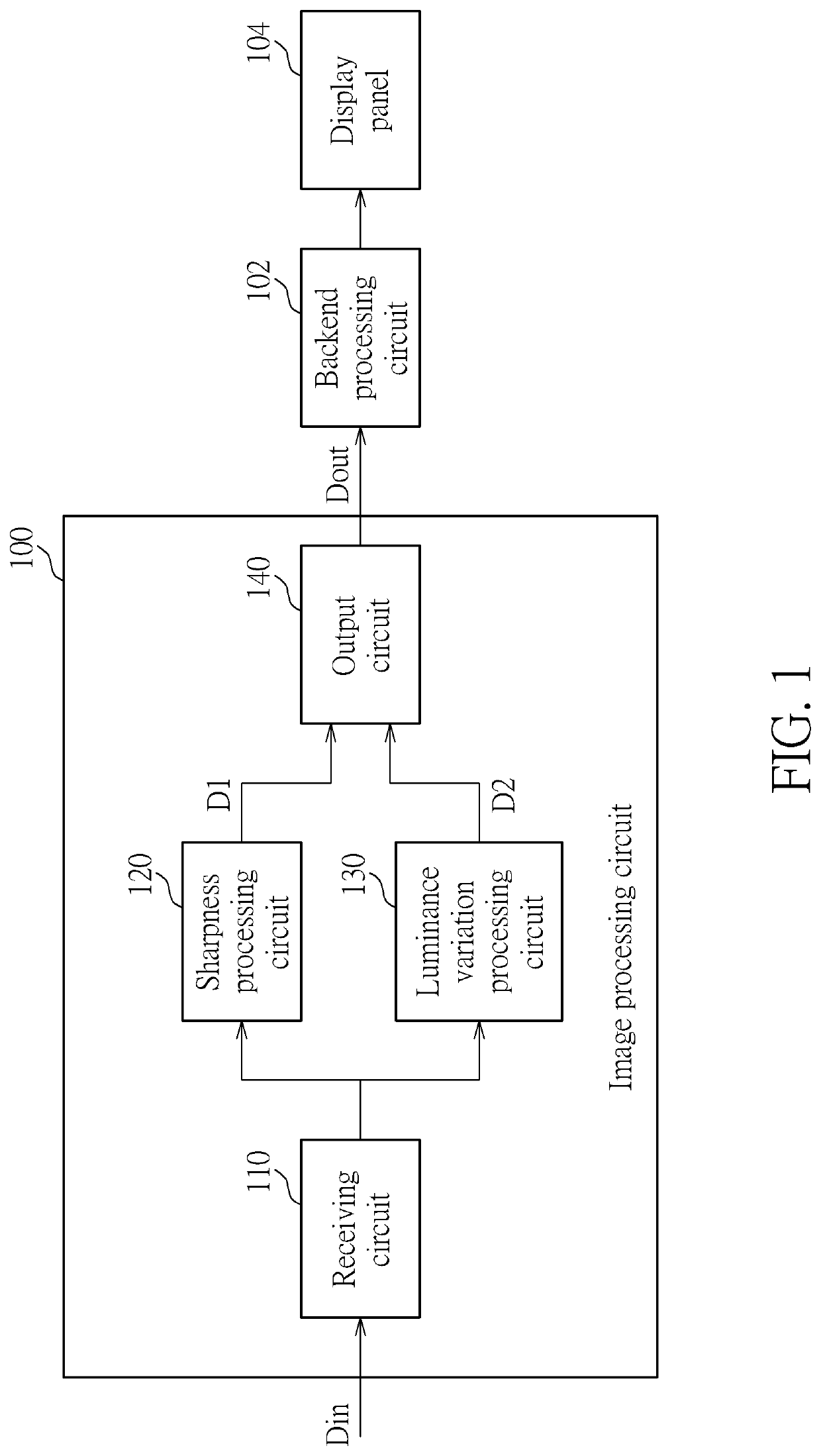
[0010]FIG. 1 is a schematic block diagram of an image processing circuit according to an embodiment of the invention. As shown in FIG. 1, the image processing circuit 100 comprises a receiving circuit 110, a sharpness processing circuit 120, a luminance variation processing circuit 130 and an output circuit 140. In this embodiment, the image processing circuit 100 is configured to receive image data (an image frame) Din and sharpen the image data to generate an output image Dout. The output image Dout maybe further processed by a backend processing circuit 102 and then provided to a display panel 104 for being displayed on the display panel 104.

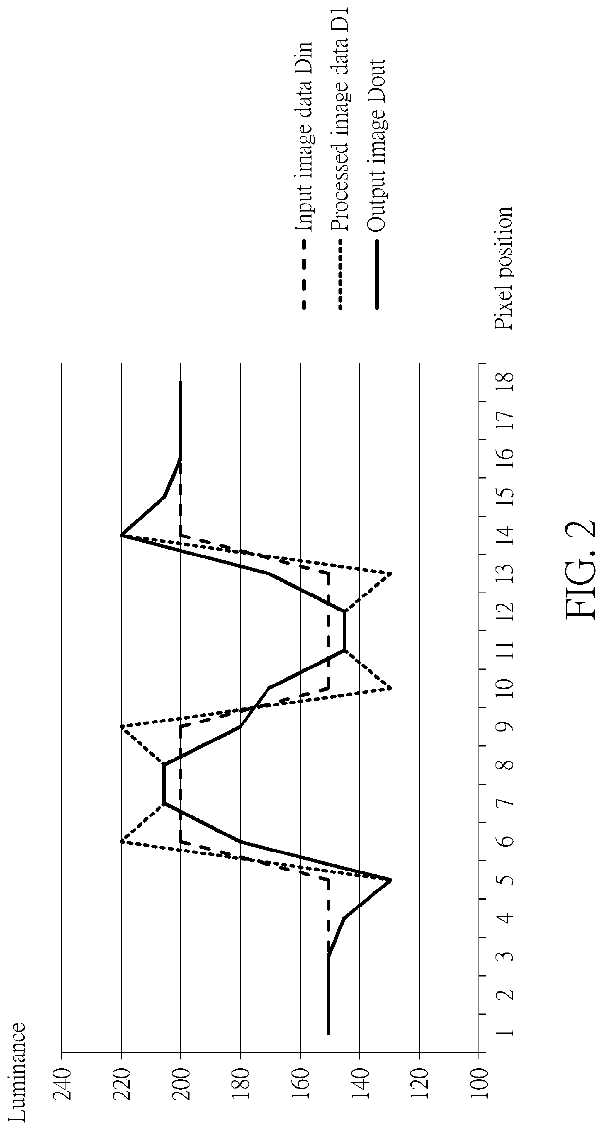
[0011]In the operations of the image processing circuit 100, the receiving circuit 110 is configured to receive the image data Din. The sharpness processing circuit 120 is configured to perform a high-pass filtering operation on the image data Din to generate processed image data D1. For example, the high-pass filtering operation may be perfo...


PUM


Abstract

The present invention discloses an image processing circuit, wherein the image processing circuit comprises a receiving circuit, a sharpness processing circuit, a luminance variation processing circuit and an output circuit. In the operations of the image processing circuit, the receiving circuit is configured to receive image data; the sharpness processing circuit is configured to perform a high-pass filtering operation on the image data to generate processed image data; the luminance variation processing is configured to determine a high frequency component of each pixel within the image data, and for each pixel, the luminance variation processing circuit is configured to calculate a difference between high frequency components of the pixel and neighboring pixel(s) to generate auxiliary image data; and the output circuit is configured to generate output image according to the processed image data and the auxiliary image data.

Description

BACKGROUND OF THE INVENTION1. Field of the Invention[0001]The invention relates to an image processing circuit, more particularly to an image processing circuit for improving sharpness of an image.2. Description of the Prior Art[0002]Conventionally, the linear high pass filter (HPF) is utilized to improve image sharpness. However, when the frequency of the linear HPF is high (or the length of the HPF is short), the original texture of the image will be damaged, resulting in that the edge luminance of an object is higher than its central luminance. In addition, when the frequency of the linear HPF is low (or the length of the HPF is long), the sharpened object becomes thicker and a thicker ringing is formed at the edge of the object, which affects the display quality.SUMMARY OF THE INVENTION[0003]In view of this, an objective of the invention is to provide an image processing circuit which can effectively improving the sharpness of the image while preventing the conventional defect f...

Claims


Application Information

Patent Timeline
Patent Type & Authority Applications(United States)
IPC IPC(8): G06T5/00G06T5/20
CPCG06T5/003G06T2207/10004G06T5/20G06T5/73
Inventor HUANG, YU-SHIANG
Owner REALTEK SEMICON CORP
Features
  • R&D
  • Intellectual Property
  • Life Sciences
  • Materials
  • Tech Scout
  • Unparalleled Data Quality
  • Higher Quality Content
  • 60% Fewer Hallucinations
Learn More