

Integrated circuit defect diagnosis using machine learning
Patent Information
- Authority / Receiving Office
- US · United States
- Patent Type
- Applications(United States)
- Current Assignee / Owner
- CARNEGIE MELLON UNIV
- Publication Date
- 2021-02-11
Smart Images
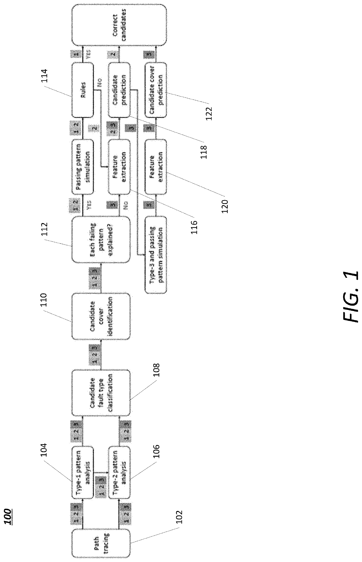
Figure 1 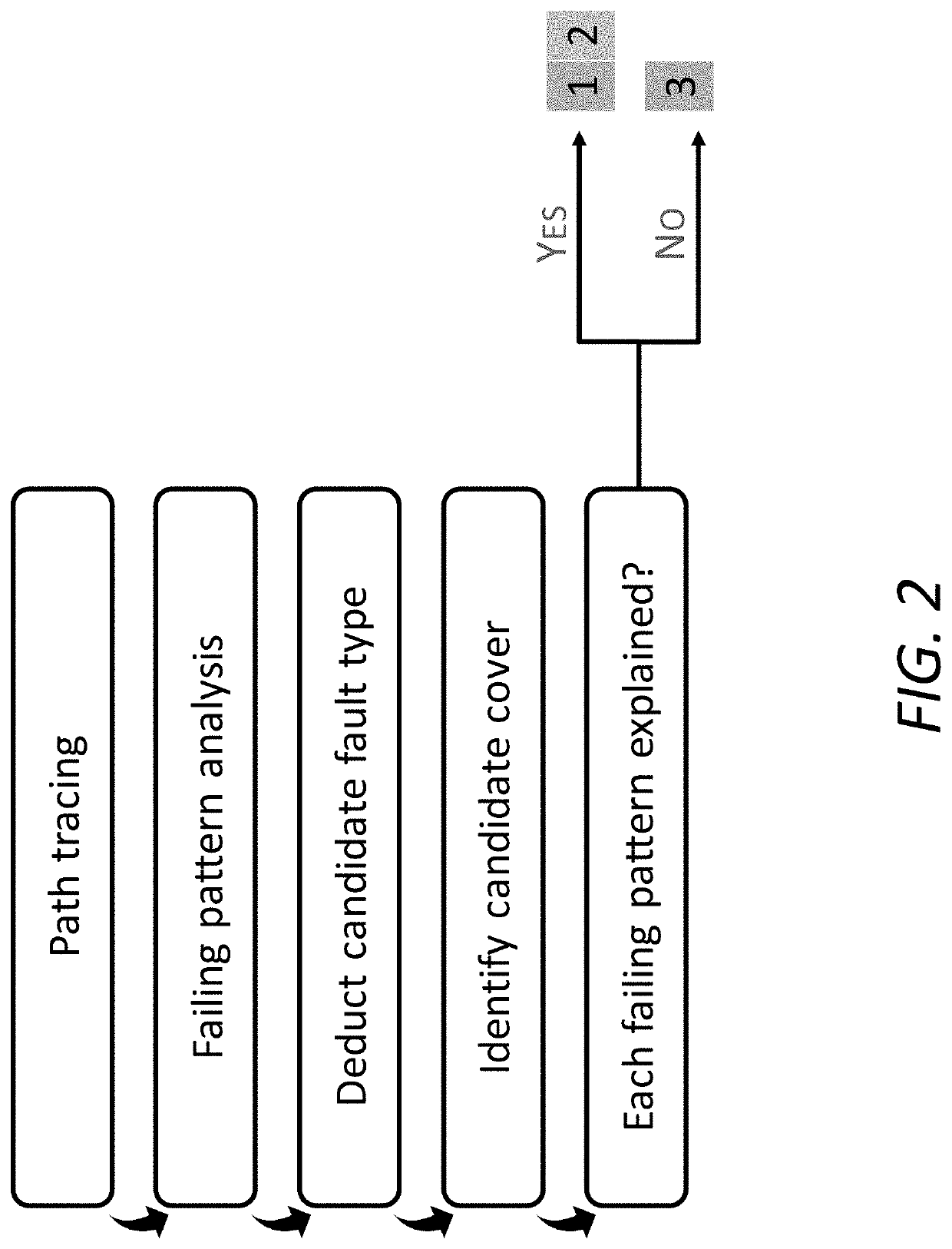
Figure 2 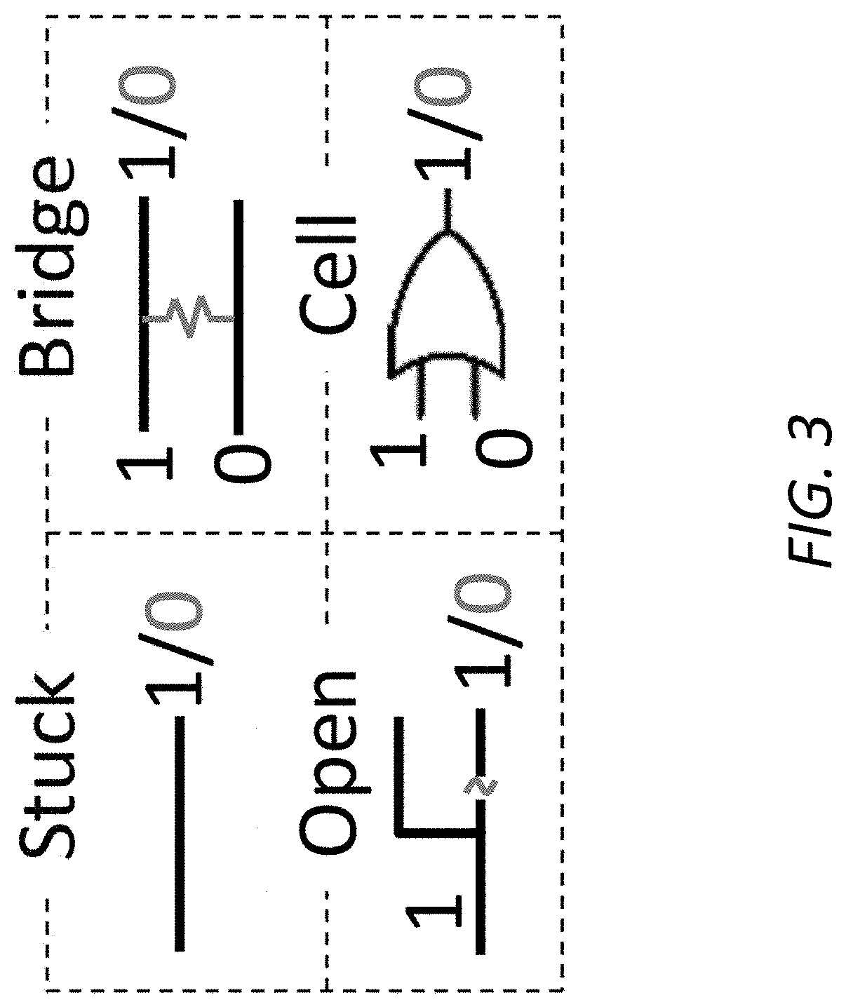
Figure 3
Abstract
Description
RELATED APPLICATIONS
[0001] This application claims the benefit of the U.S. Provisional Patent Application No. 62 / 922,401, filed Aug. 7, 2019, the contents of which are incorporated herein in their entirety.GOVERNMENT RIGHTS
[0002] This invention was made with government support under contract No. CCF-1816512 awarded by the National Science Foundation. The government has certain rights in this invention.BACKGROUND OF THE INVENTION
[0003] With respect to the manufacture of integrated circuits, yield is defined as the proportion of working chips fabricated. Yield can be relatively low when a new manufacturing process or a new chip design is introduced. The process of identifying and rectifying the sources of yield loss to improve both chip design and manufacturing is called yield learning. The rate of yield learning is extremely critical to the success of the semiconductor industry and must thus be accelerated to meet the triple objectives of diminishing time-to-volume, time-to market and t...